Hey There,
This has been a very standard doubt among students/freshers/VLSI professionals. The answer to this query is simple to explain in words and text, but was not quite satisfying to students, unless VSD Interns themselves were able to solve it last night
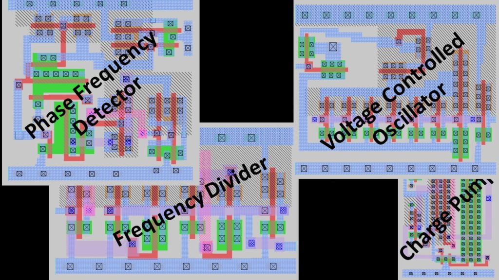
Last night during VSD Internship call, VSD interns, who were working on a critical IP’s and SoC’s using Sky130 PDK’s, came up with a unique explanation to this query of their own.
That was a moment of “wow” for VSD because it literally took 10-years to explain difference between Foundry IP’s and Macros in most beautiful and silicon-proven methodology.
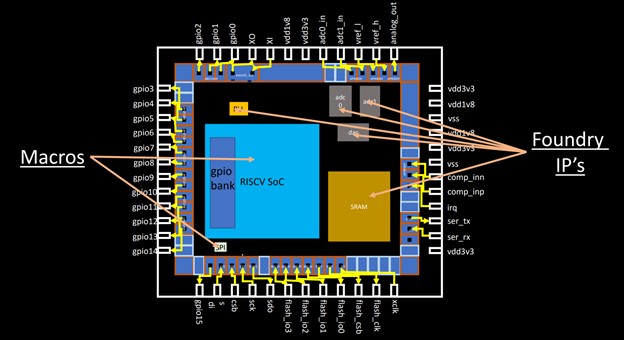
If you observe above image, it is noticeably clear about what an IP and Macro is. But with above image, comes a lot of queries like “why PLL, ADC, SRAM are really called IP’s and not macros? And vice-versa”. Now that is a problem statement, which just cannot be solved with words or text. There are 2 ways to solve this query
- Designing IP’s and using same IP for PNR
- Let students design this IP
Last year, when we did a series of VLSI SoC design workshops, we collected a list of students who were really interested in knowing the difference between IP and Macro, and this year January2020, VSD announced IP design Internship program only for students who had attended VSD workshops.
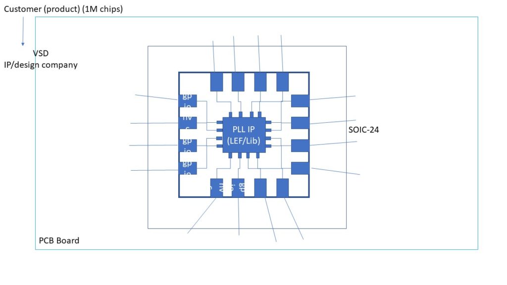
Not only were they(VSD Interns) able to build PLL IP on their own, but also came up with a test-plan to test PLL chip using a testbed and SOIC-24 package. They upgraded VSD as IP design company for understanding concepts😊. Below image is directly from our Internship call (SOIC-24 is shown as pin package for explanation purposes). GitHub Links for all below projects layout and design specifications with Sky130 will be shared soon
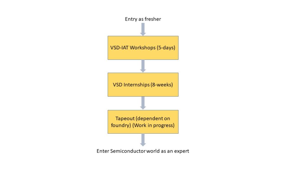
Now this is how we narrate the “journey”. A great one – not only for VSD, but also for entire VSD community. The journey has just begun, in nutshell, below image shows a well-designed VLSI Skilling model (VSD Workshops + VSD-IP design Internship + Tapeout[working on it]), which is not just participants driven but also silicon proven. To summarize, given a problem statement, VSD Interns and participants, who have gone through this rigorous training and designing model will have much better ways to figure out solutions by themselves.
The 2nd run of VSD-IAT Advanced Physical Design using OpenLANE/Sky130 workshop starts on 25th November. If you are interested in participating, below is the registration link.
All the best and happy learning !!
