Introduction To Industrial Physical Design Flow
VLSI Physical Design Flow is an algorithm with several objectives. Some of them include minimum area, wire length and power optimization. It also involves preparing timing constraints and making sure, that netlist generated after physical design flow meets those constraints.
Following section will help you to understand the very basic and beginning steps for chip design. It is exactly the way it happens in leading VLSI chip design industries.
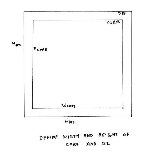 The very first step in chip design is floorplanning, in which the width and height of the chip, basically the area of the chip, is defined. A chip consists of two parts, ‘core’ and ‘die’.
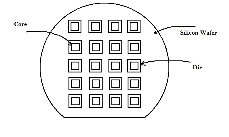
A ‘core’ is the section of the chip where the fundamental logic of the design is placed. A die, which consists of core, is small semiconductor material specimen on which the fundamental circuit is fabricated. IC’s are fabricated on a single 9 inch or 12 inch diameter silicon wafer, which contains hundreds of mirror images of the fundamental logic. This wafer is then cut into small pieces, each piece has similar functionality of the fundamental logic. This is called ‘die’
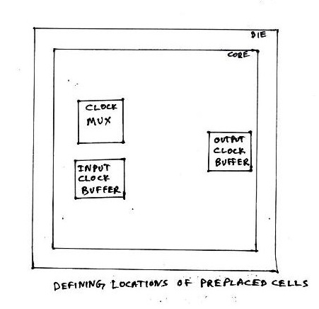
During placement and routing, most of the placement tools, place/move logic cells based on floorplan specifications. Some of the important or critical cell’s locations has to be pre-defined before actual placement and routing stages. The critical cells are mostly the cells related to clocks, viz. clock buffers, clock mux, etc. and also few other cells such as RAM’s, ROM,s etc. Since, these cells are placed in to core before placement and routing stage, they are called ‘preplaced cells’. The above diagram describes the same.
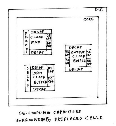
Once the critical cells are placed on the chip, it becomes necessary to surround the critical cells by decoupling capacitors. The placement of de-coupling capacitors surrounding the pre-placed cells improves the reliability and efficiency of the chip.
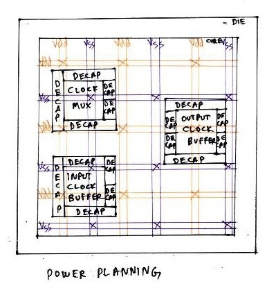
Usually, while drawing any circuit on paper, we have only one ‘vdd’ at the top and one ‘vss’ at the bottom. But on a chip, it becomes necessary to have a grid structure of power, with more than one ‘vdd’ and ‘vss’. The concept of power grid structure would be uploaded soon. It is actually the scaling trend that drives chip designers for power grid structure.
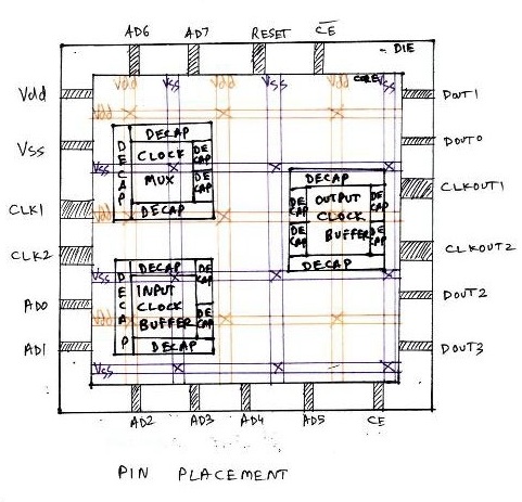
During floorplan, we define the width and height of both, core and die. The space between core and die is reserved for pin placement. For eg. an 8085 has around 40 pins viz. reset, AD0, AD1, etc.
Also, the clock pins (for eg. CLK1, CLK2, CLKOUT1, CLKOUT2 in above diagram) are wider compared to other pins on the chip. It is the clock on a chip that drives most of the logic inside the chip. Hence, it should have very low resistance, and thus wide area, as resistance is inversely proportional to area.
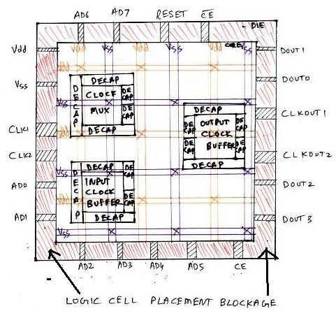
To avoid the placement of cells by placement tools, in the area between core and die (which is reserved for pin placement), it needs to be blocked by logical cell placement blockages. It is very similar to blocking a road under renovation, so that no one drives on that road, and that road is reserved for some special purpose.
Once the floorplan is freezed, it is given as an input to the placement and routing (PNR) tools. These tools are built with intelligent algorithms which would consider the design requirements (usually called as ‘constraints’) such as clock frequency, timing margin, max capacitance etc., calculate the location of the logical cells (Flipflops, AND, OR, BUFFER, etc) and place them in the floorplan. All the design requirements (or constraints) are stored in a single file called as ‘design constraints’ file, which is recognized by most of PNR tools.
Lets talk about few examples on how the built-in algorithms of PNR tools behave after detecting design constraint. The inputs to PNR tools are the design netlist, floorplan, timing libraries and design constraints.
Timing libraries is a database that stores complete information about input capacitances, timing arcs, etc. of the logical cells. It also stores the list of all logical cells of different sizes.
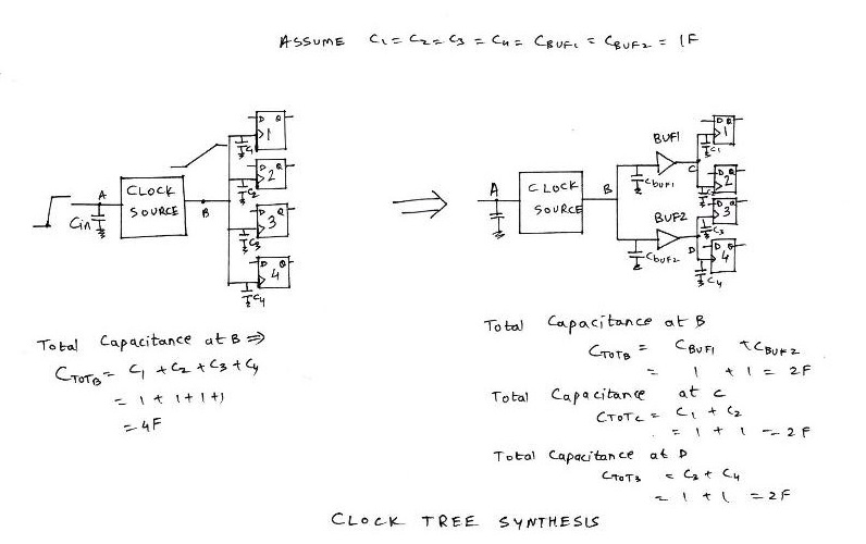
Assume, the design has a constraint which specifies that maximum capacitance on a net should not exceed 2F. Now consider the schematic in the above diagram. Clock source has a node ‘B’ which is connected to the ‘clk’ pin of 4 flip-flops. Assume that the input capacitance at ‘clk’ pin of each flip-flop is 1F. So now, the PNR tool built-in algorithm calculates the total capacitance on node ‘B’ as addition of all input capacitance’s at ‘clk’ pins of 4 flip-flops i.e 4F. Then the tool compares this capacitance number with the max capacitance constraint in the constraints file which is 2F.
Since the capacitance at node ‘B’ is exceeding by 2F, the tool divides the load on node ‘B’ through 2 buffers as shown in right side of the above figure. It selects buffers from timing library in such a way that each of those buffer has an input capacitance of 1F, and builds a tree, called as ‘clock tree’. The whole process of dividing the load on clock net is called ‘Clock tree synthesis (CTS)’. Above example is one of the scenarios that is considered during CTS.
The PNR tools looks for any special physical requirements from user other than timing constraints.
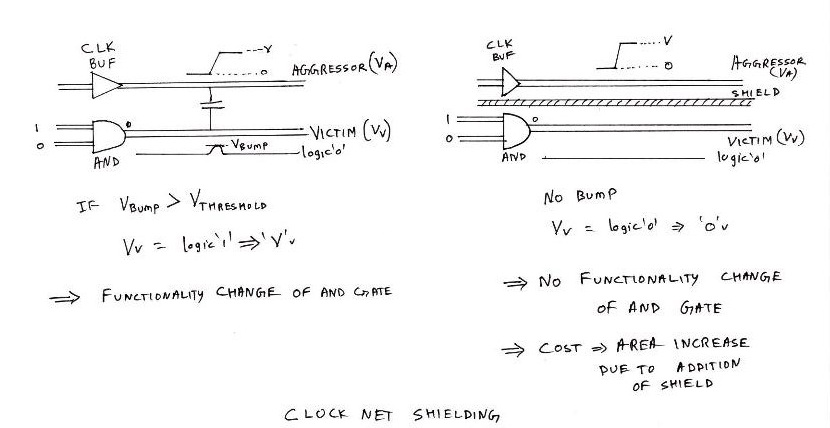
Let us create a scenario in which output net of clock buffer and output net of an AND gate are placed very close to each other, as shown in above figure. Also assume that output of AND gate is at logic ‘0’, while the clock is switching at regular intervals. Consider clock switching from ‘low’ to ‘high’. Since, the output net of AND gate is placed very close to the clock net, there is a high possibility that, during switching, the logic ‘1’ might get coupled to the output of AND gate, which causes a bump with voltage ‘Vbump’.
Since, a logic change or voltage level change on clock net, is causing a voltage level change on the nearby output net of AND gate, the clock net is called as ‘AGGRESSOR’ whereas the output net of AND gate is called as ‘VICTIM’. If the bump voltage Vbump on VICTIM exceeds a certain margin or threshold, the output of AND gate switches to logic ‘1’ which changes the functionality of the design. This phenomenon is called Crosstalk.
An efficient way to avoid the above scenario is to add a shield between VICTIM and AGGRESSOR which would break the coupling between them and hence logic level on the output net of AND gate would be retained. This requirement of adding shield around specific nets could be fed as an external input to the PNR tool. Cost paid in the above scenario would be an increase in the chip area.
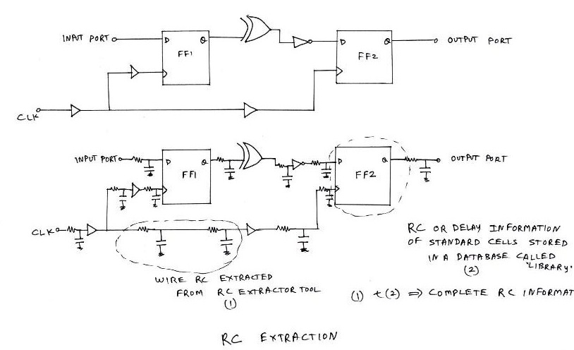
Finally when design layout is complete, the PNR tool generates a new netlist which has information about any modifications done to the original netlist, for eg. buffer addition, cell size changes, etc. It also creates a ‘definition’ file, which has the connectivity information between the logical cells, viz. wire length, width, locations, etc. This definition file is used to extract additional timing information due to wire inbuilt RC’s (resistances and capacitance’s) and store them into a separate file usually referred to as SPEF (Standard Parasitic Extraction Format) file. The design, which has the logical cells and the physical connectivity information between the cells, needs to be analysed in terms of timing i.e. the design should meet timing constraints defined by user in the beginning of PNR. Plugging the SPEF information to logical design (which is the new netlist generated by PNR tool), the complete timing information of the design is fed as an input to any Static Timing Analysis (STA) tool.
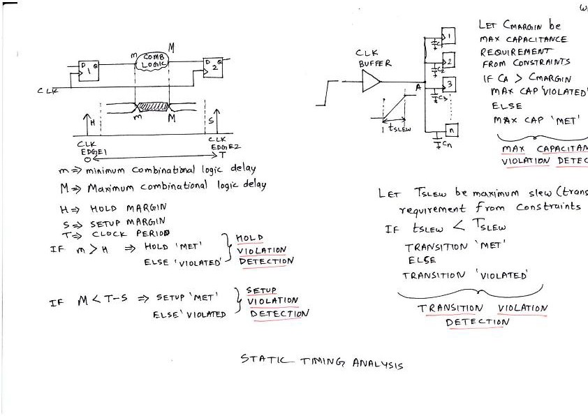
Static Timing Analysis (STA) tool helps to identify specific paths in the design which fail to meet timing requirements specified in the constraint file. These failing paths are flagged as ‘VIOLATED’. There are 4 kind of checks for which the design is tested viz. Setup check, Hold check, Max Capacitance check and Transition Check. Above figure displays the scenarios under which the timing analysis tool will flag or detect violations. Once these violations are detected, it becomes necessary to analyse these violations, and plug the fixes to these violations back to the PNR netlist. This process of fixing violations by modifying the routed PNR netlist is referred to as Engineering Change Order (ECO).
