Kunal Ghosh, the visionary co-founder of VLSI System Design (VSD) Corp. Pvt. Ltd., stands at the forefront of online open-source EDA and hardware design education, particularly in the realm of RISC-V.
With a portfolio of 50 top-tier VLSI online courses, Kunal has enriched the learning journey of over 90,000 students across 153 countries. His expertise extends beyond training; he’s actively involved in pioneering open-source projects and design collaborations with esteemed institutions like IIT Madras, IIT Bombay, IIT Guwahati and IIT Hyderabad.
His current focus is on crafting high-quality open-source Analog/Digital IPs, a groundbreaking endeavor in open-source hardware design. Kunal’s rich industry experience includes roles at Qualcomm and Cadence, specializing in SoC design. He holds a master’s degree from IIT Bombay, where he specialized in VLSI & Nano-electronics, with a focus on sub-100nm Electron Beam Lithography Optimization techniques.
Timothy Edwards, Founder Opencircuitdesign.com and SVP at Efabless.He is Analog VLSI designer and collecting and developing open-source EDA tools for over 27 years, He worked for the Johns Hopkins Applied Physics Lab, startups MultiGiG and Analog Devices. He has developed open-source EDA software tools such as Magic, Qflow, Netgen, and Xcircuit.
Mohammed Shalan, Associate Professor, American University in Cairo.He is Founder of CloudV.io, The Open Cloud-based Digital ASIC/FPGA Design Environment, Fault, the only open-source DFT solution. He worked as Embedded Systems Architect for Automotive and Mobile (Mentor Graphics), Embedded Software Manager (MindSpeed and Mentor Graphics), Digital ASIC Designer (Freescale), SoC Consultant, Digital ASIC PnR Consultant.He holds Patents- Power Profiling for Embedded System Design, Power System Optimization and Verification for Embedded System Design.
Ahmed Ghazy, fresh Computer Engineering graduate from the American University in Cairo with a minor in Mathematics. Currently working at eFabless where he worked on the OpenLANE flow 1 for over a year now and made many contributions to open-source EDA tools including the OpenROAD tools, magic, and netgen.Other research interests include computer security and cryptography, data structures and algorithms, and combinatorics.
VSD Launches VSDSquadron In Collaboration With IIT Madras & DIR-V

Job Roles, Convergence With Embedded Systems, and Startups
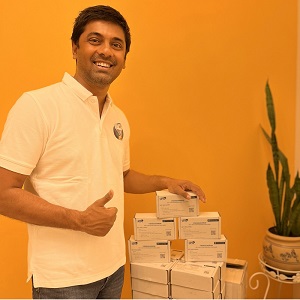
VSD showcased at Semicon India 2023

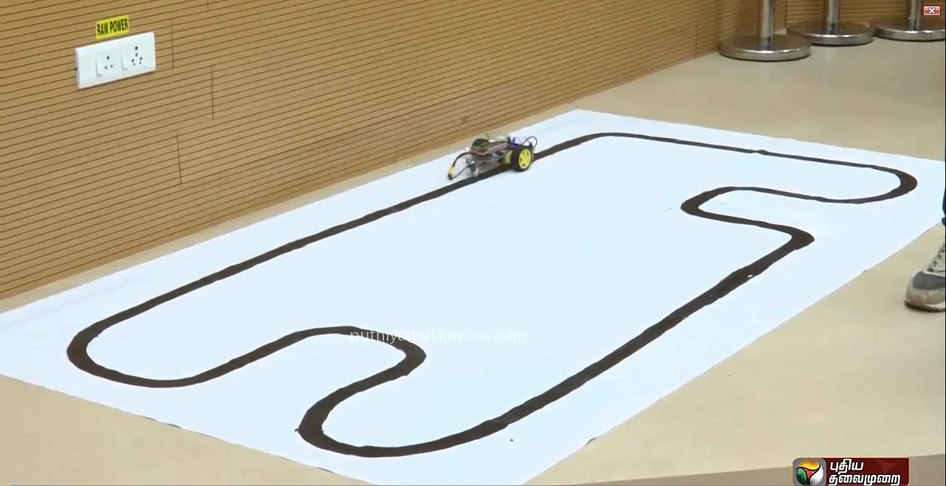
VSDSquadron Educational board on Tamil News channel
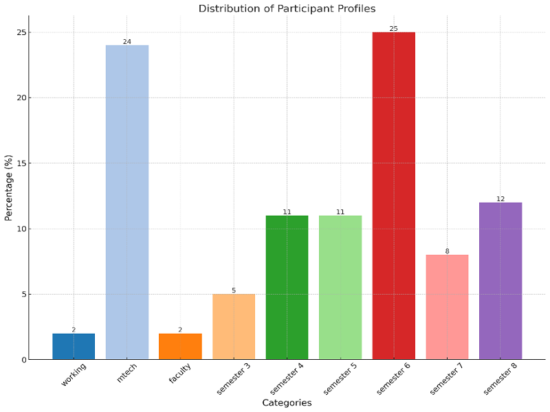
5 Day Workshop on VLSI Design Flow using RISCV and EDA Tools
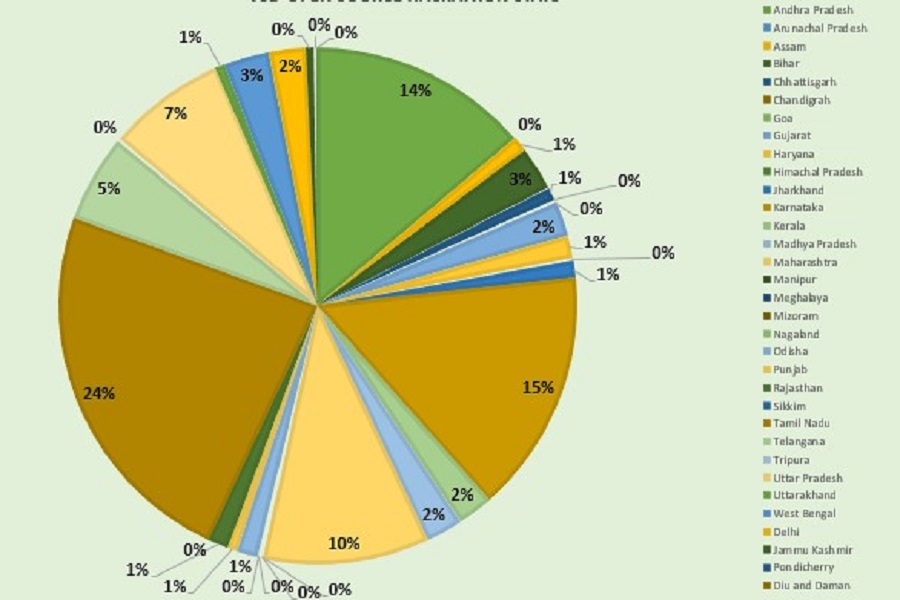
Karnataka VLSI roadshow at Sahyadri College, Mangalore
