That’s because it takes 18 transistors to design it….
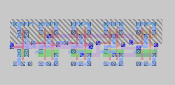
The above image is a layout of a D-flipflop which I designed from scratch, i.e. from inv to nand to D-flipflop. And you will find all files in below github link:
https://github.com/kunalg123/flipflop_design
But the question then you should be asking me is – Why did I design this? Well, if you look it from basic concepts and from “first principle” point of view, it has so many things for you to learn and get started with “Standard Cell design”, which is by far the most popular and demanding field as it deals directly with foundry
Did you realize the first gate is an INVERTER, and the next 4 gates are NAND?
Things to learn from this (and reasons I find this horrible, other than the 18 transistors it takes)–
- Power rail discontinuity – We would like to have continuous power rail
- N- and P-diffusion discontinuity – We would like to have continuous diffusion. For my Physical design friends, remember, we add “FILLER” cells at the end of routing, and you always wondered why we are doing so.
- Small substrate contacts – Except for inverter, all substrate contacts are single width, which will create high resistance path for current, thus increasing “Clk-to-Q” delay
- Hanging metal1 – If you see for the NAND gate outputs, there is lot of hanging metal1
Now you see why I find this horrible….If you find more reasons, please email….I know 7 more reasons for this one to be a bad design
This gives you a chance, to download all files from github, modify them, play around with them and come up with the best flipflop design.
Now, even though this flipflop was badly designed, I went ahead and characterized it with SPICE and below is what I got:
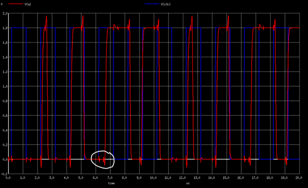
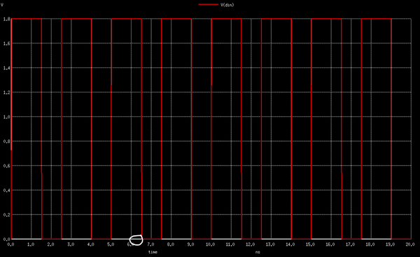
Except for clock rise edge at 6.3ns and 16.3ns (see first image for clk), at all other rising clock edge, it violates setup time. Why? Because we except the data at ‘Q’ to be stable, once captured with rise-edge of flip-flop. But for every other clock edge, the ‘Q’ varies, except at 6.3ns and 16.3ns.
This gives a “library setup time” of 477ps, which is quite a “typical” number for 180nm technology node. Now that will happen in characterization, irrespective of whether design is horrible or not, because we are still characterizing
In conclusion, there are many things to learn even from the worst design you have ever made. And FYI – I have corrected my design, reviewed it from experts and got their sign-off. But I have not uploaded it, as I want you to use this as starting point
Here’s the github link again:
https://github.com/kunalg123/flipflop_design
All the best
Happy designing and learning…
