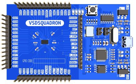
Category Archives: Floorplan


Ever heard of Chip Design Pentagon?
Know what Pentagon is? It is a plane figure which has 5-straight sides and 5-angles. For a perfect pentagon, it needs all its sides and angles to be the same, till the last decimal. Do you know what is the similarity between pentagon and our upcoming workshop “Advanced Physical Design workshop using OpenLANE/SKY130”? Look above image and you would guess it right. It is a perfect blend of topics where even a fresher can jump-start his/her career in chip design in just 5-days

6th mile-stone in field of open-source – FREE VLSI tool installation course
A full-fledged video lectures on step-by-step process to install OpenLANE EDA tool chain and Sky130 PDK open-process on your own laptop, from scratch. There is a dependency on vsdflow, though for fresh users and with Windows or fresh Unix machines. To do something like this, it needs a clear focus on end vision, with very good VLSI fundamentals, which demands hours of efforts every day

5th mile-stone in field of open-source – another compact SRAM
This time its @Reuel did a pretty great job of building a pretty compact 6T-SRAM cell and he is just a third year engineering student

2nd mile-stone in field open-source (open-lane EDA + Google/Sky130)
@Nickson joined our research project group under VSD Research internship program which runs for 8-weeks. He was supposed to develop flow for standard cell design and characterization using all open-source tools – magic/ngspice, then plug those standard cells into open-source PNR flow by open-lane, and benchmark RTL2GDS flow results. This needed a knowledge, not only of PNR, but device physics, custom layout, DRC/LVS and then (finally) Physical design/STA.

‘Made in India’ SHAKTI processor on VSDFLOW – Now that’s exciting
With learning being online, SHAKTI core and ‘vsdflow’ being opensource, this is first-time in the history of VLSI design & EDA (thanks to RISC-V ecosystem and Shakti Team at IITM lead by Prof. Kamakoti), a chip will ever be taped-out using all open source flow, which will cater to almost 80% Indian Semiconductor Market.

Paper 2: PNR for digital core IC to pads using Cloud based eda tool
A simple chip frequency divider but most prominently used in counter modules of a microproceesor or as standalone IC can be completely designed from Verilog code to layout . A complete chip with IO pins and labels on it can be designed with help of efabless cloud based eda tool just like a commercial IC. There are two toolbox in efabless one is CloudV for Verilog or c code & other is Open Galaxy for backend design for designing commercial like IC with zero cost involved & same can be given to Semiconductor foundries for mass production. From Preparation , synthesis to DRC cleanup using Q flow manager a Core part of IC can be obtained with log files of each stage used in this process. A innovative feature of interactive DRC under Magic tool enables the designer to rectify DRC violations on the spot. Moreover, ESD protection is also available under Opengalaxy tool for use of chip in electrosensitive applications.

Symposium III – Floorplanning of digital IC’s for best area
This blog is regarding abstract submission for VSDOpen2018, which is the first online conference in VLSI, that covers all aspects of semiconductor technology with prime focus to build SoC using RISC-V CPU by illustrating exciting ways using (only) opensource EDA tools.

Can you approve my floorplan?
Just to give you some background, picoSoC is an example SoC using PicoRV32, and PicoRV32 is a size-optimized RISC-V CPU which implements RV32IMC instruction set architecture.

The Perfect Launch – By Kunal and Rajeev
We launched industry grade PNR EDA tool ‘Proton’ on web in front of 100 people across 7 countries, which I think, by far, has been a perfect launch for any partial open-source EDA tool.The below link has the details of the launch:
https://www.udemy.com/vsd-physical-design-webinar-using-eda-tool-proton/