The Power of an Intense VLSI Program by SFAL/VSD

Today, as technology races towards ever-smaller geometries and more complex chips, the need for professionals who are not just well-versed in theory but also skilled in practical, hands-on experience has never been more critical. An intense VLSI program that mirrors industry practices is the beacon that guides aspiring engineers across this bridge.

The Journey through EDA Tools in Chip Design

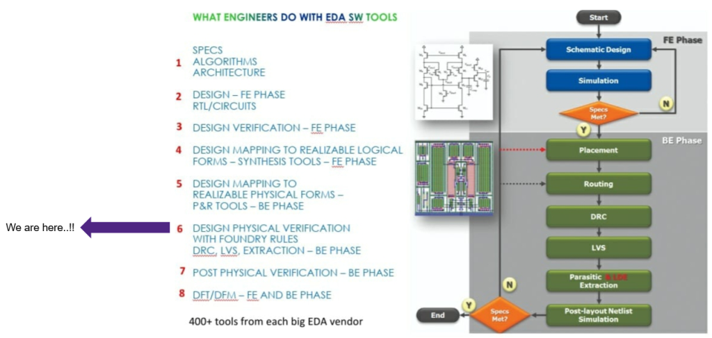
The above image encapsulates the structured journey an engineer traverses in the landscape of chip design using EDA tools. It underscores the sequential phases of chip design, beginning with the conceptualization of specs and algorithmic architecture. Progressing through the Front End (FE) phase, the focus shifts to the intricate tasks of design and verification, where engineers translate Register Transfer Level (RTL) descriptions into logical circuits. As the pathway advances, it reaches a crucial juncture—mapped in the image as the current location—where designs are transformed into physical forms through Placement & Routing (P&R) tools in the Back End (BE) phase. This meticulous progression is indicative of the comprehensive scope an engineer needs to master, from synthesis to post-physical verification, ensuring the design is fully prepared for the tapeout phase. This illustration vividly outlines the crucial benchmarks of chip design, delineating the vast array of over 400 tools available from prominent EDA vendors, thus highlighting the depth and complexity of the field.

Synopsys’ Verification Process

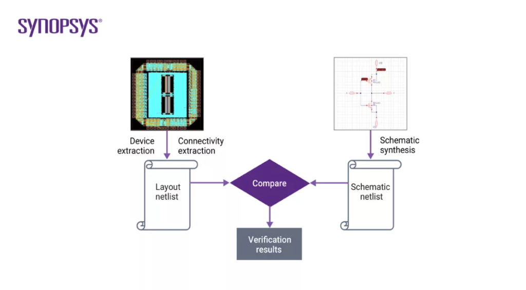
In this image, Synopsys presents a refined focus on the verification phase of chip design, illustrating the essential steps of ensuring the layout’s fidelity to the original schematic. The process initiates with device and connectivity extraction from the physical layout, leading to the generation of a layout netlist. Concurrently, schematic synthesis yields a corresponding schematic netlist. These two netlists then undergo a rigorous comparison, ensuring that the schematic intentions are accurately translated into the physical layout. This step is pivotal in the design flow and is reflective of the meticulous attention to detail required in the verification process. It serves as a testament to the importance of precision in the design of integrated circuits, and the verification results serve as a quality checkpoint before proceeding to subsequent stages.

CMOS Inverter Design Rules

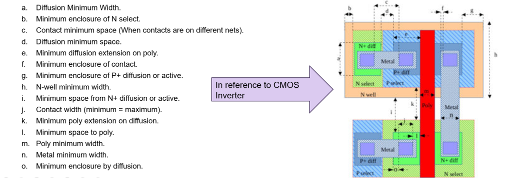
The third image is a deep dive into the world of design rules specific to a CMOS inverter—a fundamental building block in digital circuits. It lists the myriad of parameters, such as minimum widths and spacings, that are vital to the physical realization of semiconductor devices. Each rule corresponds to the geometrical and topological constraints of the CMOS inverter’s layout, ensuring that the device will not only be manufacturable but also perform reliably. This layout adheres to stringent design rules such as diffusion widths, spacing between contacts, and the enclosure requirements for various layers. The adherence to these rules is paramount in avoiding fabrication failures and ensuring the inverter’s functionality. This image provides an invaluable reference for engineers, distilling the essence of complex fabrication design rules into a comprehensive visual guide.

Correcting Design Rule Violations

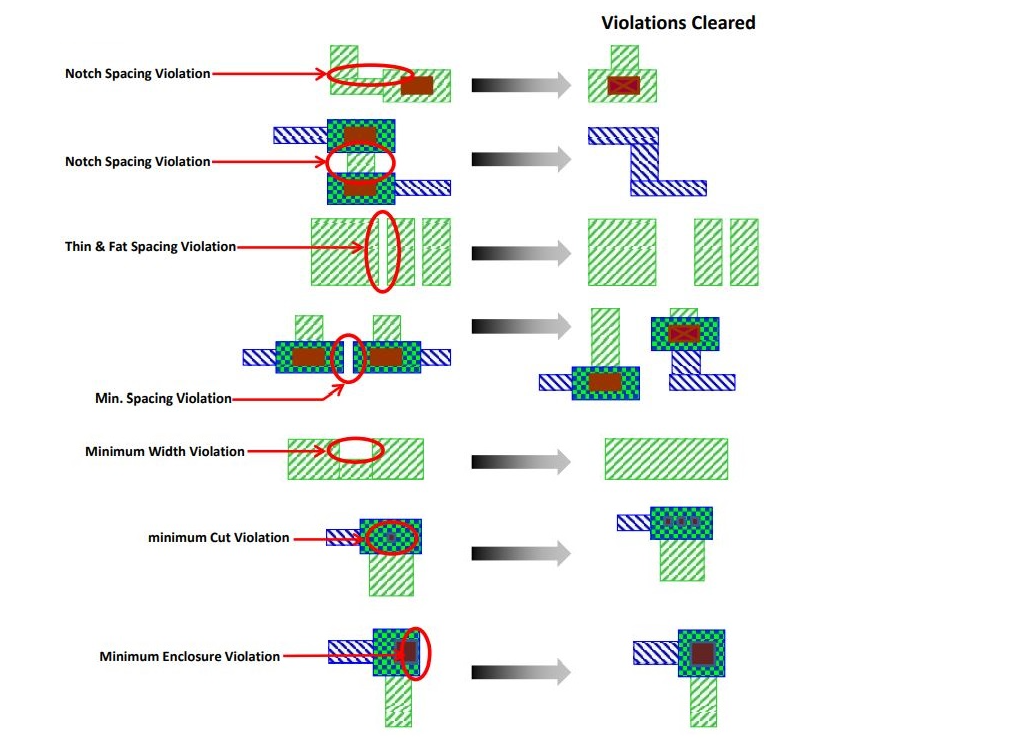
This image vividly portrays the iterative process of identifying and correcting design rule violations, a critical aspect of ensuring a manufacturable chip. Displaying common DRC violations, such as notch spacing, thin and fat spacing, and minimum width constraints, it illustrates the corrective actions necessary to adhere to the stringent standards of integrated circuit design. This step-by-step resolution of errors demonstrates the practical challenges faced during the layout phase and the importance of DRC in the VLSI design process. The image reinforces the continuous loop of validation and refinement that is essential to achieving a defect-free design, indicative of the high-quality standards maintained in the semiconductor industry. It serves as a stark reminder of the complexity and precision required in the chip fabrication process, and the relentless pursuit of perfection that defines the field.
SFAL-VSD Program link

Registration for Ethical RISC-V IoT Workshop

Welcome to Ethical RISC-V IoT Workshop

The “Ethical RISC-V IoT Workshop” at IIIT Bangalore, organized in collaboration with VSD, is a structured, educational competition aimed at exploring real-world challenges in IoT and embedded systems. Participants progress through three stages: building an application, injecting and managing faults, and enhancing application security. The event spans from May 9 to June 15, 2024, culminating in a showcase of top innovations and an award ceremony. This hands-on hackathon emphasizes learning, testing, and securing applications in a collaborative and competitive environment.

Rules :
  1. Only for Indian Student whose college is registered under VTU
  2. Only team of 2 members can Register
  3. Use only VSDSquadron Mini resources for product development
Awards :
  1. Prize money for final 10 Team
  2. 3 Winner team’s Product will be evaluated for Incubation
  3. 7 consolation prizes
  4. Completion Certificate to final round qualifier
  5. Chance to build a Proud Secured RISC-V Platform for India

Date for Registration : 9th May - 22nd May, 2024
Hackathon Inauguration : 23rd May 2024

VSDSquadron (Educational Board)

VSDSquadron, a cutting-edge development board based on the RISC-V architecture that is fully open-source. This board presents an exceptional opportunity for individuals to learn about RISC-V and VLSI chip design utilizing only open-source tools, starting from the RTL and extending all the way to the GDSII. The possibilities for learning and advancement with this technology are limitless.

Furthermore, the RISC-V chips on these boards should be open for VLSI chip design learning, allowing you to explore PNR, standard cells, and layout design. And guess what? vsdsquadron is the perfect solution for all your needs! With its comprehensive documentation and scalable labs, thousands of students can learn and grow together.

VSD HDP (Hardware Design Program) Duration-10 Week

With VSD Hardware Design Program (VSD-HDP),  you have the opportunity to push the boundaries of what exist in open source and establish the new benchmark for tomorrow.

It will leverage your degree in Electrical or Computer Engineering to work with

  • Programmable logic
  • Analog/ digital IP
  • RISC-V
  • Architecture & microprocessors
  • ASICs and SoCs on high-density digital or RF circuit cards
  • Gain hands-on knowledge during design validation and system integration.

Sounds exciting to just get started with expert mentors, doesn’t it? But we are looking for the next generation of learners, inventors, rebels, risk takers, and pioneers.

“Spend your summer working in the future !!”

Outcomes of VSD Online Research IP Design Internship Program

  1. Job opportunities in Semiconductor Industry
  2. Research work can be submitted to VLSI International journals
  3. Participate in Semiconductor International Conference with Internship Research Work
  4. Paper Publications in IEEE Conference and SIG groups
  5. Tape out opportunity and IP Royalty
  6. Interact with world class Semiconductor designer and researchers
  7. Academic professions where more research projects are encouraged.
  8. All the above research and publication work will help colleges and institutes to improve accreditation levels.

Know More Information

VSD – Intelligent Assessment Technology (VSD-IAT)

VSD – Intelligent Assessment Technology (VSD-IAT) is expertly built training platform and is suited for designer requirements. Semiconductor companies understand the value of training automation and Engineer performance enhancement, and do not need to be convinced of the impact of a virtual platform for learning. VSD trainings are quick, relevant, and easy to access from any device at any time zone.

VSD Intern Webinars

VSD Interns made it happen !!

VSD is working towards creating innovative talent pool who are ready to develop design and products for the new tech world. VSD believes in “Learning by doing principle” , and always prepare the student to apply the knowledge learned in the workshops, webinars and courses. We always push our students to work on new designs, test it and work continuously till it becomes the best performing design. Any student who enrolls to VSD community starts working with small design and grows with us and develops a tapeout level design with complete honesty and dedication towards the Work !!

Check out VSD Interns Achievement!

VSDOpen Online Conference

Welcome to the World’s only online conference in Semiconductor Industry VSDOpen Conference. With enormous support and global presence of audience from different segments of industrial lobby and academia made a highly successful event. Evolution is change in the genetic makeup of a population over time, online conference is one kind evaluation everyone adapt soon. 

  • VSDOpen 2022 is an online conference to share open-source research with the community and promote  hardware design mostly done by the student community.
  • VSDOpen 2022 is based on the theme “How to lower the cost to learn, build, and tapeout chips ?”  , which will provide a platform to community to build stronger designs and strengthen the future of Chip design.
  • VSDOpen is envisioned to create a community based revolution in semiconductor hardware technology.
  • The open source attitude is required to bring out the talent and innovation from the community who are in remote part of world and have least access to the technologies.  And now Google support will help to bring the vision to execution by VSD team

VSD Online Course by Kunal Ghosh

VSD offers online course in complete spectrum of vlsi backend flow from RTL design, synthesis and Verification, SoC planning and design, Sign-off analysis, IP Design, CAD/EDA automation and basic UNIX/IT, Introduction to latest technology – RISC-V, Machine intelligence in EDA/CAD, VLSI Interview FAQ’s.

Current Reach – As of 2021, VSD and its partners have released 41 online VLSI courses and was successfully able to teach  ~35900 Unique students around 151 countries in 47 different languages, through its unique info-graphical and technology mediated learning methods.

Enquiry Form