What I did in 8-weeks-VSD Internship? – Bandgap v1
I worked on designing a General Purpose Band-Gap reference circuit with N-Well Resistors in 180nm CMOS process technology with a temperature coefficient of 26.26 ppm/°C, VDD=3.3V and Vbgp=1.2056V. The internship required us to use only Opensource Tools from start to finish, and at the end, we released our designs to the Opensource community
Before delving into technical details on the Band-Gap Reference, it is necessary to understand what it does and what significance it holds in Chip Design.
What is a Band-Gap Reference and Why is it important?
A general purpose band-gap reference circuit should generate a reference voltage, ideally independent of temperature, supply voltage, load and process variations.
Why is it important?
An on-chip band-gap reference is a crucial block in the design of analog integrated circuits as the accuracy and precision of these circuits can be limited by the reference voltage. BGR blocks are used in data converters-ADCs & DACs, LDOs, DRAMs, encoders & decoders, signal processing blocks, sensor interfaces, and several other applications. Therefore, a designer should take care to design a BGR circuit with a high power supply rejection ratio and an extremely low temperature coefficient.
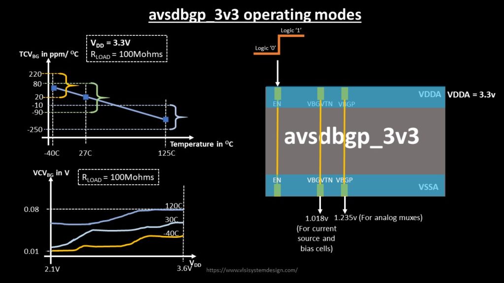
Post-Layout Performance Characteristics of the designed Band-Gap Reference Circuit
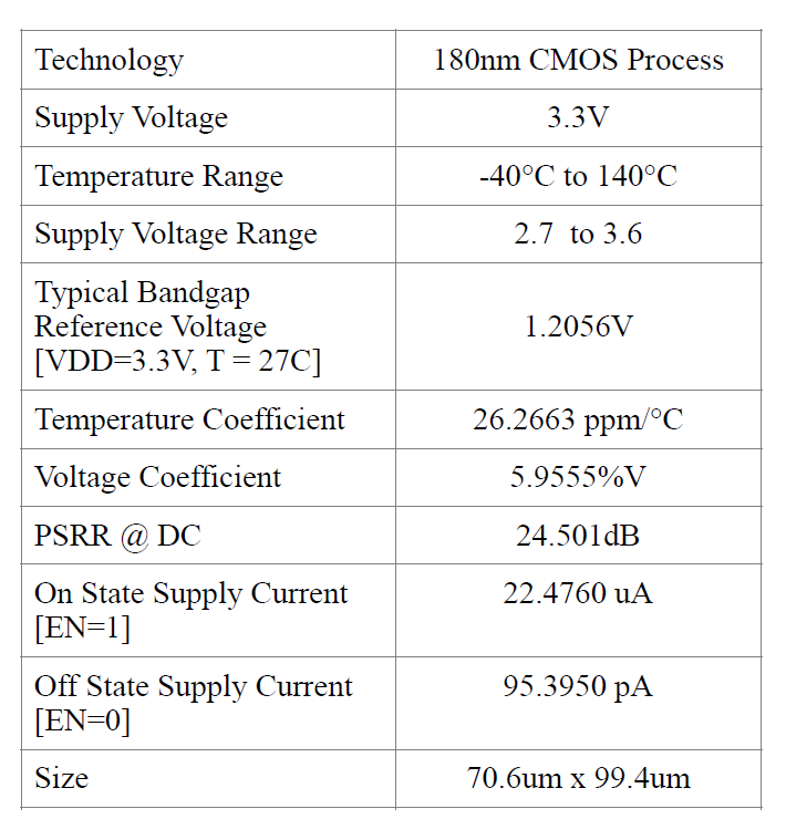
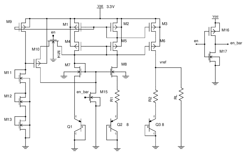 Fig. 1 Circuit Diagram of BGR Circuit
Circuit Design:
The bandgap reference voltage is generated using PTAT and CTAT references. A cascode current mirror is employed in the bandgap reference circuit formed by M1, M2, M3, M4, M5, M6, M7, M8. The CTAT current is generated in the branch with Q1 and the PTAT current is generated in the branch with Q2 and R1. The PTAT current is driven into R2 and Q3, developing a PTAT voltage drop across R2 and a CTAT voltage drop across Q3, the summation of the voltage drops generates the reference voltage, which can be scaled using R1, R2 and n, no. of BJTs connected in parallel. As a self biased cascode current mirror is used, using a startup circuit is imperative to prevent it from going into the zero current state. M9, M10, M11, M12, M13 form the startup circuit. If the cascode current mirror enters the zero current state, M10 is turned on and it provides a discharge path for the gate nodes of PMOS in the current mirror, forcing the self- biased current mirror to enter into the normal operation state, after which M10 is turned off. A power down circuit is also formed using
M14, M15, when the enable signal is HIGH, M14 is turned on and M15 is off, when the enable signal is LOW, M14 is off, disabling the start-up circuit and M15 is turned on, proving a direct path to ground from the NMOS gates of the current mirror, hence switching it off.
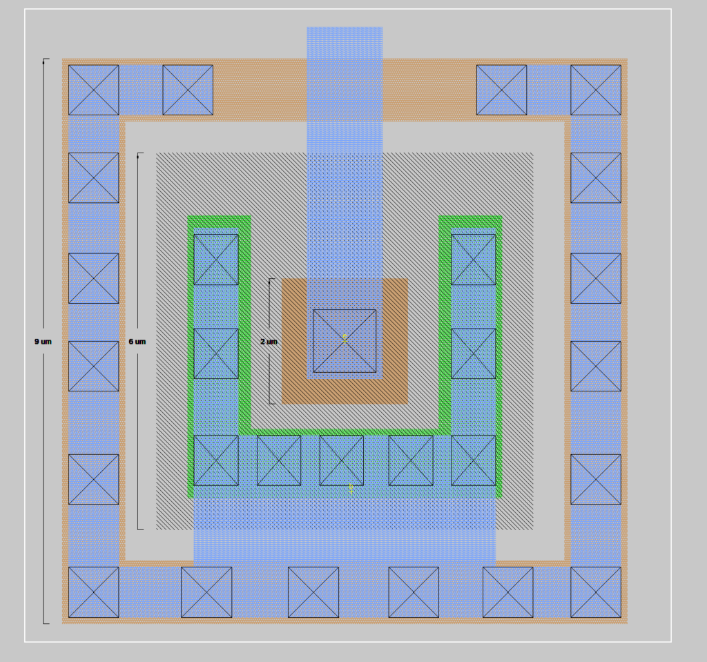 Fig 2. Layout of Vertical Parasitic PNP BJT
 Fig 3. Layout of Nwell Resistor using Serpentine Structure
 Fig 4. Layout of Nwell Resistor using Serpentine Structure
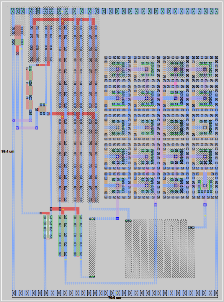 Fig 5. Layout of Nwell Resistor using Serpentine Structure
Layout:
In the CMOS Technology process, the diode is implemented as a vertical parasitic PNP BJT. The PNP BJT is in the diode connected form, with the collector and base tied together. The p+ implant acts as the emitter, the nwell with the n+ in it behaves as the base, and the p+ in the p-substrate behave as the collector. A diode is formed between the p+ implant and nwell. 17 diode connected BJTs are required for the for designed bandgap reference circuit, and 3 additional BJTs are used while laying out the BJTs according to the Common Centroid Matching Pattern. The Matching can be further improved by surrounding the BJTs with additional dummy BJTs. In the current layout, no matching technique has been employed for the current mirror.
Future Work & Potential Improvements:
1. Improved matching techniques such as Common Centroid / Interdigitisation need to be implemented while laying out the current mirror.
2. Corner Analysis Testing of the bandgap reference circuit is yet to be performed.
3. The load driving capability needs to be improved by addition of a buffer block such as an OTA or a common drain amplifier.
4. To adjust the reference voltage resistors must be trimmed using fuses, hence, resistor trimming must be employed in the circuit.
5. The design must be improved to provide a higher PSRR.
6. In the future an OTA based bandgap reference circuit will be developed with improved performance characteristics. Also, a second order bandgap reference will be studied and designed, to improve the temperature coefficient.
An in-depth documentation of the designed Band-Gap Reference circuit can be found here:
https://github.com/sherylcorina/avsdbgp_3v3
 Refer below link to know more about VSD-IAT workshops and future internships:
https://www.vlsisystemdesign.com/vsd-iat/
