What I did in 8-weeks-VSD Internship? – Graph Extractor from Spice Netlist & Euler Path Generator
The Problem — (Circuit to Layout Conversion)
No. of Foundries → TSMC,GF,Intel,Samsung, UMC etc. As the technology scales down, all these foundries release their versions of PDK and these PDKs are different for different foundries.
Standard Cell Layout Generation → Characterized Std Cells are required for the PnR process. Every time the tech node changes, the Char. Engineer/Layout Engineer has to draw the circuits for the basic std cells and lay it out individually. This is a time consuming process. (Given the exorbitant no. of cells ). The idea is to automate the std cell layout generation for various std. Cells.
Existing Projects (Active) —
ALIGN → (Analog Layouts Intelligently Generated from Netlists) — This is a collaborative project by UMinn (Sachin Sapatnekar), TAMU and Intel Labs, Oregon funded by DARPA. (https://github.com/ALIGN-analoglayout/ALIGN-public)
MAGICAL → (Machine Generated Analog IC Layout) — This is a collaborative project by UT-Austin (David Z Pan) and is financed by DARPA. (https://github.com/magical-eda/MAGICAL

This idea was extremely hard for me to implement.
Reasons —
- I did not have the expertise on Graph Theory.
- I did not have expertise on Tech Mapping.
- The philosophy of generating layouts was not based on Euler Tours. (I am still unsure of the idea to generate Analog Layouts.)
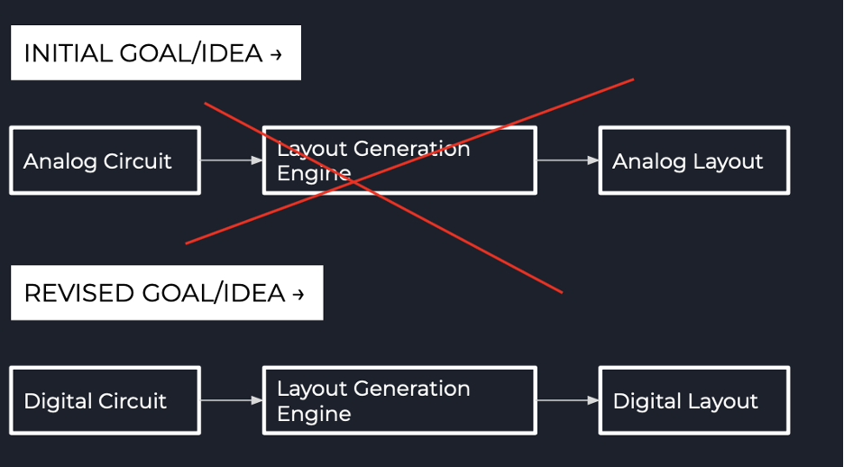
We then pivoted to generating Digital Layouts. Although there are Digital Layout Generators available, we tried to get some hands on developing the project.
Existing Projects (Digital Layout Generator) —
LC Layout — Libre Cell Layout. Developed by ETH-Zurich. (https://codeberg.org/tok/librecell)
Conventional Approach —
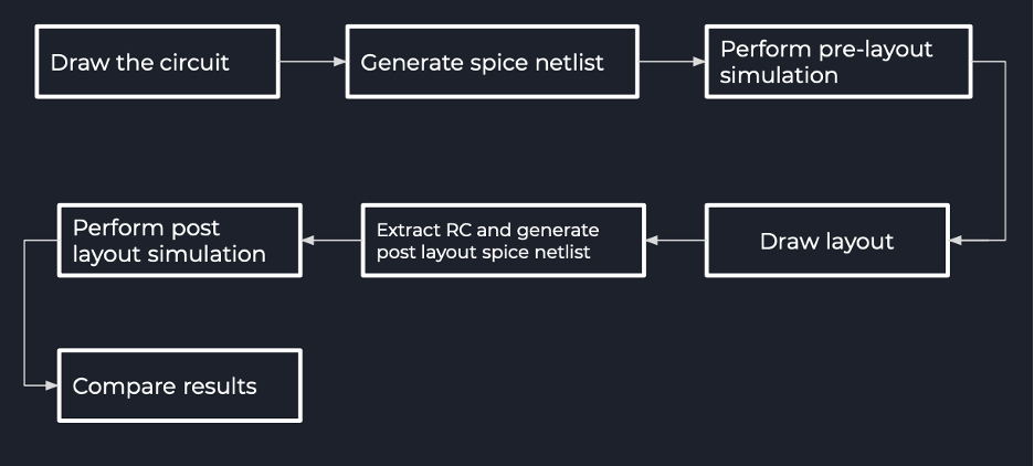
Context — We are working with Digital Circuits.
Proposed Approach —
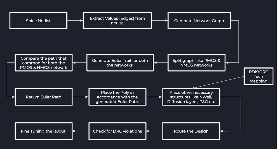
Challenges —
- Tech Mapping.
- Graph Splitting.
- Integrating DRC Rules.
- Routing
Why Euler Paths ??
Euler Path gives us the optimal way to place the poly so that there is no discontinuity in P and N diffusion layers, to avoid congestion and unnecessary over usage of routing resources.
LAYOUT WITHOUT EULER’S PATH →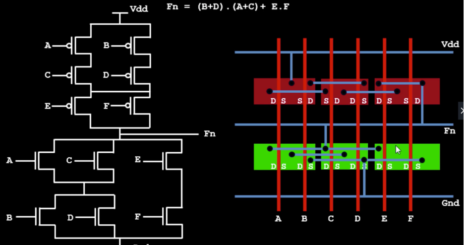
LAYOUT WITH EULER’S PATH →
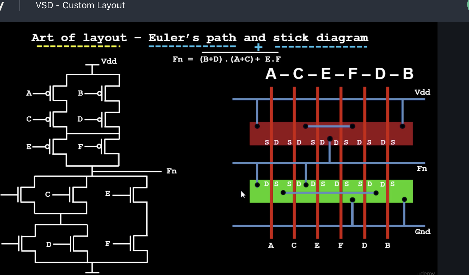
Comparison–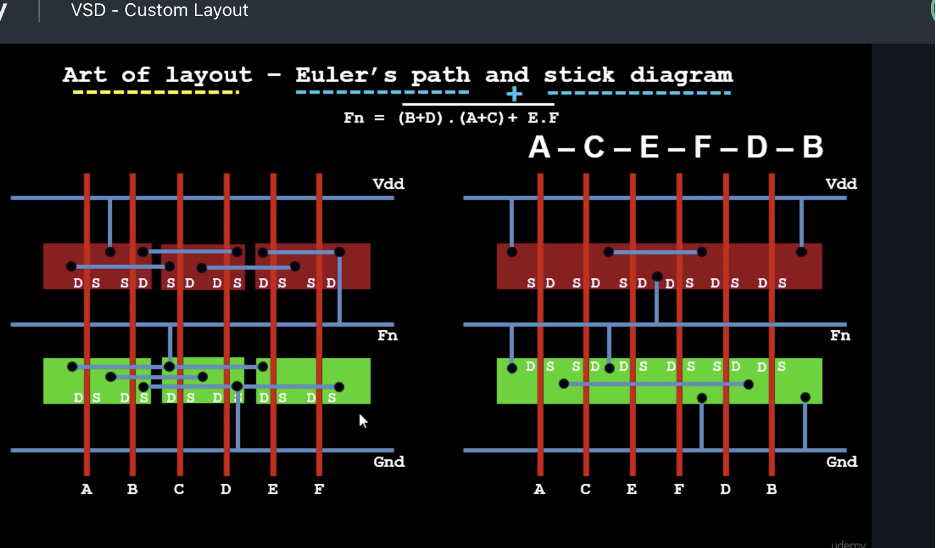
Euler Path — Eulerian Path is a path in a graph that visits every edge exactly once. Eulerian Circuit is an Eulerian Path which starts and ends on the same vertex. (https://www.geeksforgeeks.org/eulerian-path-and-circuit/) Eg.
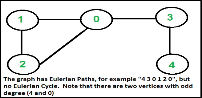
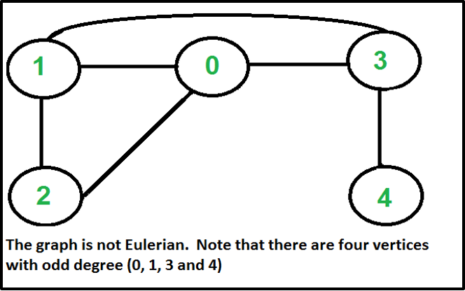
How to find whether a given graph is Eulerian or not?
The problem is the same as the following question. “Is it possible to draw a given graph without lifting a pencil from the paper and without tracing any of the edges more than once”.
*****
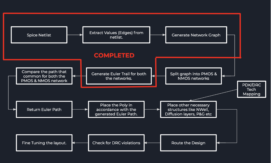
We were successfully able to generate the Euler Paths for the complete circuit. However, we needed to generate the Euler Path that is both common for both the PMOS and the NMOS logic.
Steps —
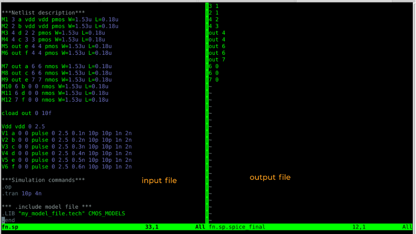
- We wrote a script to extract the relevant information from the SPICE Netlist.
Idea — There is a graph G(V,E). The transistors are converted as edges on the graph and the connections in the circuits are converted as vertices on the graph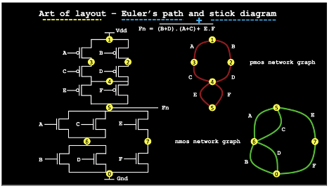
- There is some post processing that needs to be done after we get the previous output. (I need to think out some logic for that).
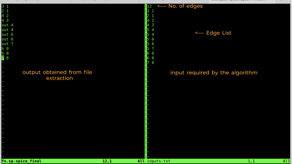
Here (3 1) denotes node 3 and node 1 are connected and (5 7 ) means node 5 and node 7 are connected in the graph.
- This file is to be fed into our Algorithm that traces the Euler Path. (Sample Output)

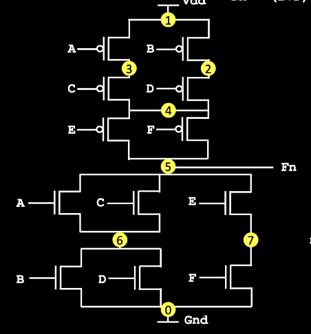
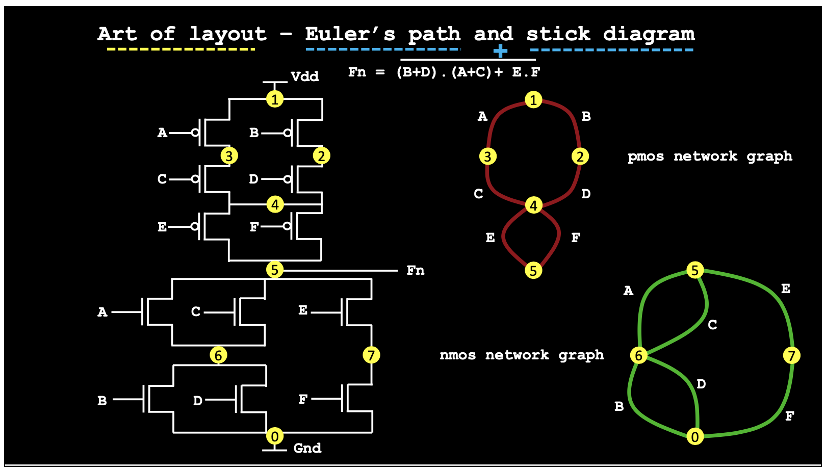
Reference Circuit for Verifying the Euler Path —
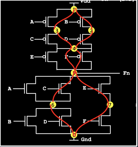
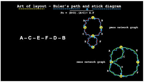
- This Algorithm however returns the Euler Path for the overall circuit. We need a common Euler Path for PMOS and NMOS circuit. (Shown Below). The Algorithm still needs some work to be carried out. Given below is the expected output.
Pending Work —
- The file conversion needs to be worked upon.
- Graph Splitting. Need to go through this. It’s very important. As of this moment, the algorithm only returns the Euler Path for the Combined (PMOS + NMOS) graph.
- Layouting for the given PDK’s seems to be a very hard task. (Tech Mapping)
- Routing the Layout. (This seems to an extremely difficult task mainly because it is done after placing the poly’s in the design)
- Pass Transistor. Layouting for pass transistor logic is a bit complicated as it requires adding dummy nodes/edges and forming the graph.
- Random Graph Generator (This is important for testing the algorithm)
- To know more about bridges and articulation points in a graph.
- I need to solve a lot of problems and get to know about some advanced concepts like Dynamic Programming and Memoization applied on graphs.
Detailed Reference and Source Code can be found here — (https://github.com/sethupathib/vsdGraphExtractor)
![]()
Refer below link to know more about VSD-IAT workshops and future internships:
https://www.vlsisystemdesign.com/vsd-iat/
