Hi
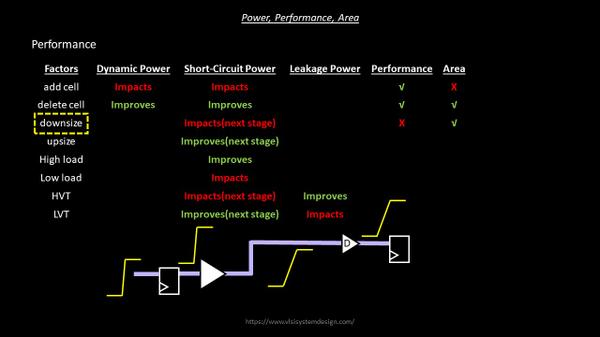
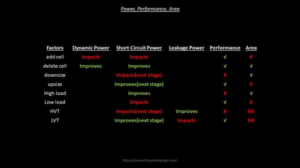
A PPA card like the above, is something which every VLSI engineer should be carrying like a business card. Why? Right from RTL to synthesis to PNR to signoff, we do things like upsize, downsize, VT swap, and many more, and all these factors impacts or tweaks your design PPA in one way or the other.
Let’s take an example of ‘downsize’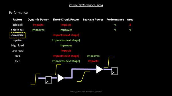
If you look at above circuit, there is a buffer towards the capture flop ‘d’ pin is strong enough to drive a small net in front of it. So, there is an opportunity over here to downsize it, thereby improving area.
Sounds simple and a great idea to a normal VLSI engineer. Now, let’s look it from an expert’s eagle eye. Investigate below image, to see what happens when you downsize a cell:
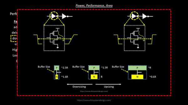
While you downsize a cell, it means, the drive strength of that cell is reduced, which impacts the RC time constant considering PMOS internal resistance (R) and output load (C). This in turn increases the output slew, as shown in left of above image.
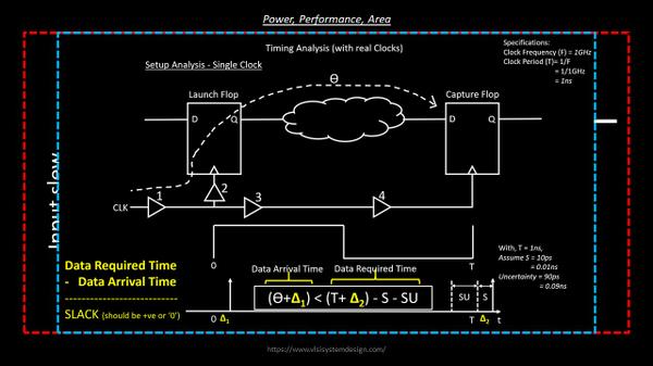
Increasing the output slew (with constant next stage output capacitance) has 2 impacts. One, more the output slew, more is the input slew of next stage, which impacts next stage delay, thus increasing the data arrival time, and hence degrading the frequency (Performance) achieved by the entire circuit, as shown in below image:
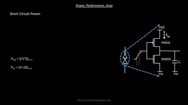
Two, due to increase in slew, the amount of time, for which your PMOS and NMOS are ON simultaneously, has increased, there by allowing current flowing from Vdd to Gnd for longer time, which impacts short-circuit current (hence sort circuit power) for next stage. Short circuit current equations and concept shown on below image:
Though, what seemed to be an easy switch from normal size to downsized cell, for a normal VLSI engineer, it seemed complex and tricky for an expert VLSI engineer. So an expert will optimize the whole process of downsizing a cell as shown below, which will still impact power (next stage) and performance, but to a minimal level.