Hi
The above image is what we had committed in 2011, when we started the company. There was a heap of challenges when we started to realize the entire flow shown in image. To name a few challenges, there was lack of tools, lack of content, lack of people who wanted to help. That’s when we were on ground ZERO
I can tell you, it was really a tough job to rise from ground ZERO and reach the above flowchart. Thanks to many people, students, professionals and mentors who have been continuously a part of this journey. I am friends with almost all of them and guarantee a huge return of investment of their precious time they spent with me
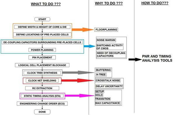
Coming to the above image, the flowchart is what you need to understand just to be an expert in the field of VLSI and semiconductors. Every topic shown in above image is a field, and every topic has a beautiful physics behind it, which when blended with tools in a video course, becomes a master-piece
The first 2 blocks which is Floorplanning and Power planning (blocks connected with first top orange and blue arrows) are encapsulated in below courses:
The third block which is clock tree synthesis, that covers buffering and h-tree, are covered in below courses:
The fourth block about clock net shielding (very important for lower nodes) is covered in below signal integrity course:
The fifth block regarding static timing analysis is extensively covered in below 3 courses:
Last but not the least, the sixth block on engineering change order is covered in below course:
The above courses should give you a very good insight about the entire flow.
Once you start or finish learning the above courses, there is an intense curiosity which rises, about how things started in VLSI or what is the basic building block of all above steps, which drives all of them. And that’s when you would need in and out understanding of MOSFETS:
https://www.udemy.com/vlsi-academy-circuit-design/
https://www.udemy.com/vlsi-academy-circuit-design-part2/
Next curiosity rises (when you do STA), that how does the internals of timing models and IP’s look like or what a macro internally has. And you would need the below course:
https://www.udemy.com/vlsi-academy-library-characterization-part-1/
https://www.udemy.com/vlsi-academy-custom-layout/
Now everyone in semiconductor industry needs to prototype and implement their ideas in a short time, which can be done with a ton of scripting languages, most popular of them is TCL scripting:
https://www.udemy.com/vsd-tcl-programming-from-novice-to-expert/
https://www.udemy.com/vsd-tcl-programming-from-novice-to-expert-part-2/
This is when you can be marked as an ‘EXPERT’ in this field. Just share all the above certificates with any company you are working with or applying for interviews
You can also go a level up, i.e., increase your skill set to the next level, by learning VLSI from architecture level, and nothing can be a best bet than learning computer architecture from scratch:
Be sincere, be persistent and be smart…. Things will fall in line
Connect with me in case you get stuck somewhere, and happy learning
