…and that’s exactly the perception that I am determined to solve.
People in my physical design course have had a glimpse of design rule check (DRC) step as a part of physical design flow, where I had mentioned that I will get back to DRC concepts. Well, I did…. in my newly (pre)launched course on ‘Custom Layout’. Let me walk you through few snippets of how to code, verify and correct drc in a custom layout. The similar concept can be propagated towards complete chip layout
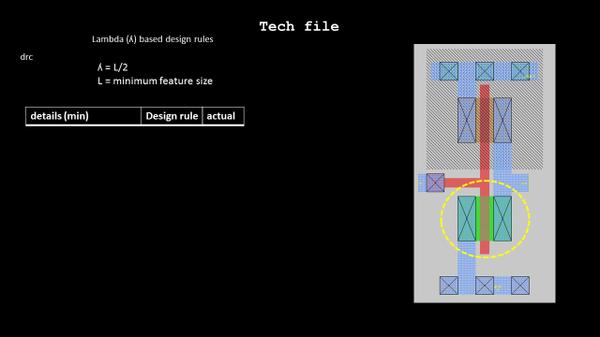
I will not use any ‘node’ specific rule so as to avoid any proprietary or legal issue (which, by the way, is more complex problem than drc, to solve :)), I will use ‘lambda’ based design rules. So lambda, as shown in below pic, can be formulated as L/2, where L is minimum feature size (any node).
Let’s look how to code a basic rule for polysilicon width. Here I create a table with ‘minimum width’, ‘design rule’ and ‘actual width’ columns. I will fill it with some values, first, then I will code it in tech file. Let’s take an example of minimum polysilicon width to be ‘2lambda’.
So, I will fill the 2nd and 3rd column as ‘2lambda’ and code it in tech file with something like below syntax
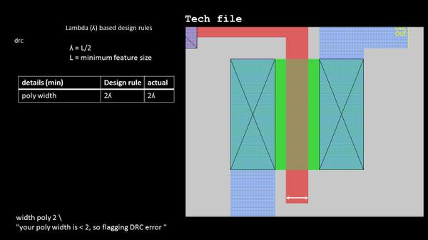
The syntax is easy to interpret…. it says, min width of poly is 2 (lambda is the units) and if min drawn width or actual width is less than 2, the error message “your poly width is < 2, so flagging DRC error” will be flagged.
This complete rule goes under the drc section of tech file something like below:
drc
width poly 2 \
“your poly width is < 2, so flagging DRC error ”
end
Now the interesting part.. when you load MAGIC layout tool (which is an open source tool I have been using to do practical layout examples in the course) with the tech file having the above drc rule coded, MAGIC tool will honor the rule, and if designer violates the rule, he will get an error message plus the area on layout for which the error is being flagged, like below:
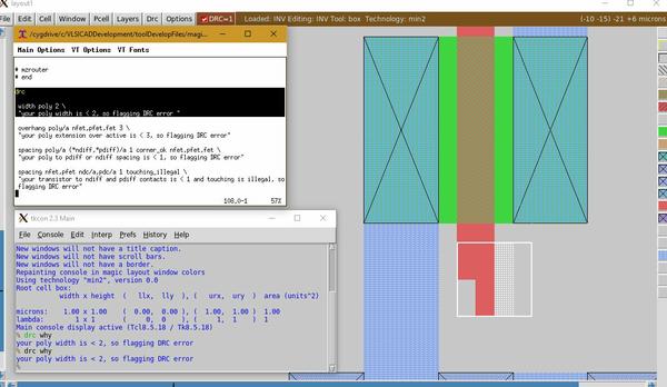
If you look into right bottom in above image, you will notice that a small section of poly silicon layer violates the rule of 2lambda, which is coded in tech file (look into drc section highlighted in tech file on top left of above image). Now to identify for designer, that this is a violation, MAGIC tool helps you with an error white dots shown in cursor box in above layout bottom right. While keeping the cursor box over the area of violation, and typing the command ‘drc why’ in MAGIC console, shown in bottom left of above image, you will see the reason why its DRC violated. Its the same message that you coded in tech file
Isn’t that “FREEDOM” to code your own DRC rules and use them in your own layout tool? Now you have full control over your design and nothing can stop you from experimenting and innovating…and that’s exactly what I have covered in my course on custom layout….
“Innovation happens when people are given the freedom to ask questions and the resources and power to find answers” — Richard Branson
Now you have everything you need…a FREE layout tool, a METHOD to code and learn your own drc rules, and an AWESOME COURSE which helps you explain how you do all of above….
So what the wait for!!!
Get in and INNOVATE!!!
