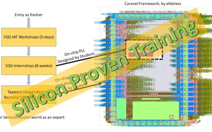
The training, the internship and finally, the tape-out – VSD Silicon proven model
A dream and a mission statement that was framed 10 years back by VSD and efabless (or let us say, e-fabulous) has now taken a […]

A dream and a mission statement that was framed 10 years back by VSD and efabless (or let us say, e-fabulous) has now taken a […]
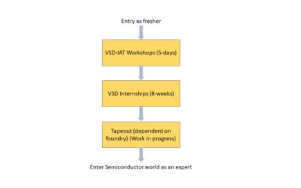
A great one – not only for VSD, but also for entire VSD community. The journey has just begun, in nutshell, below image shows a well-designed VLSI Skilling model (VSD Workshops + VSD-IP design Internship + Tapeout[working on it]), which is not just participants driven but also silicon proven. To summarize, given a problem statement, VSD Interns and participants, who have gone through this rigorous training and designing model will have much better ways to figure out solutions by themselves.
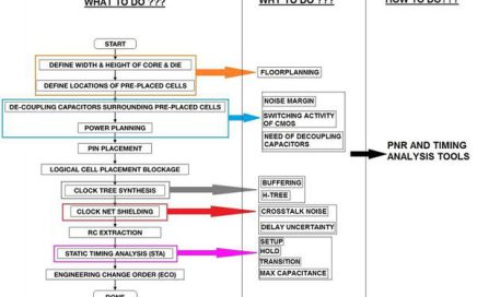
the flowchart is what you need to understand just to be an expert in the field of VLSI and semiconductors. Every topic shown in above image is a field, and every topic has a beautiful physics behind it, which when blended with tools in a video course, becomes a master-piece
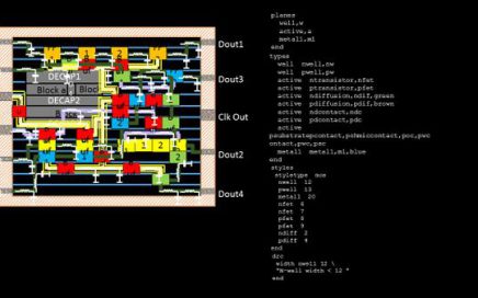
hello And that’s what I aim in my new course (yet to be released) Let me try to give you a basic snapshot of what […]
Hello, And that’s what I aim in my new course (yet to be released) Let me try to give you a basic snapshot of what […]