A dream and a mission statement that was framed 10 years back by VSD and efabless (or let us say, e-fabulous) has now taken a surprisingly good shape and IS FINALLY SILICON PROVEN. Release of Google/Skywater-130nm open PDK’s was really the final piece of entire VLSI training model puzzle.
For freshers and professionals looking forward to entering serious VLSI training business, let me put it in simple words. Remember in college, when we learned a concept in theory sessions, there was this natural curiosity to see the concepts implemented in real electronics labs using resistors, breadboards, 555 timers and so on. Similarly, in VLSI industry, there is a saying “Is It silicon proven?” Now, “it” can be IP or EDA tool or a full chip
This is where a question arises 10 years back, can VLSI trainings also be Silicon proven? Because anything on silicon brings out real problem statements, just like proving a concept on breadboard or proving an IP on silicon.
IT TOOK 10 LONG YEARS TO ANSWER THIS QUESTION AS A “YES”
Why? There were few challenges. Below were top 3-
First, you need a lot of structured, non-proprietary silicon proven content, something which VSD and its industry partners took close to 6 years to built from scratch.
Second, you need a lot of license free open-source EDA tools and labs for every detailed concept mentioned in content. efabless is equally visionary enough to take care of this part in a parallel world
Third, you need open-source designs and analog IP’s which needs to be built from scratch. This is quite challenging and (believe me) the toughest of all. Thanks to RISC-V, we managed to get open-source designs. But open-source analog IP’s? Grrrr…… None, on this whole planet earth
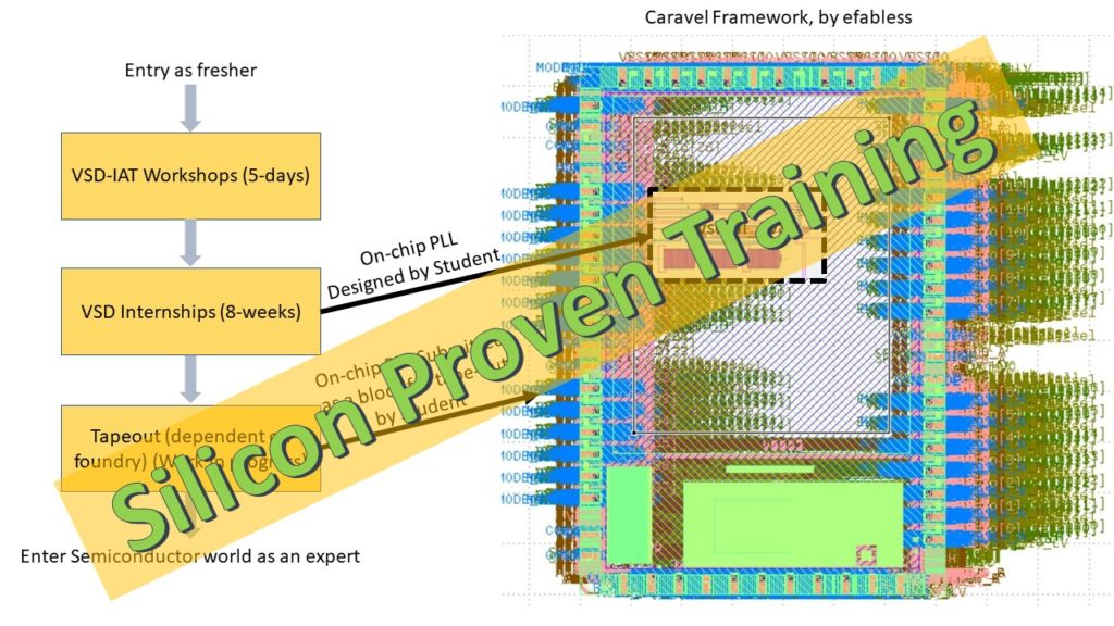
Now comes the structuring part. You must have seen below image in one of my previous posts, few weeks back, where we brought up a discussion about IP versus Macros and how it took 10 years to solve this query. This is how the entire “Silicon Proven VLSI Training” looks like
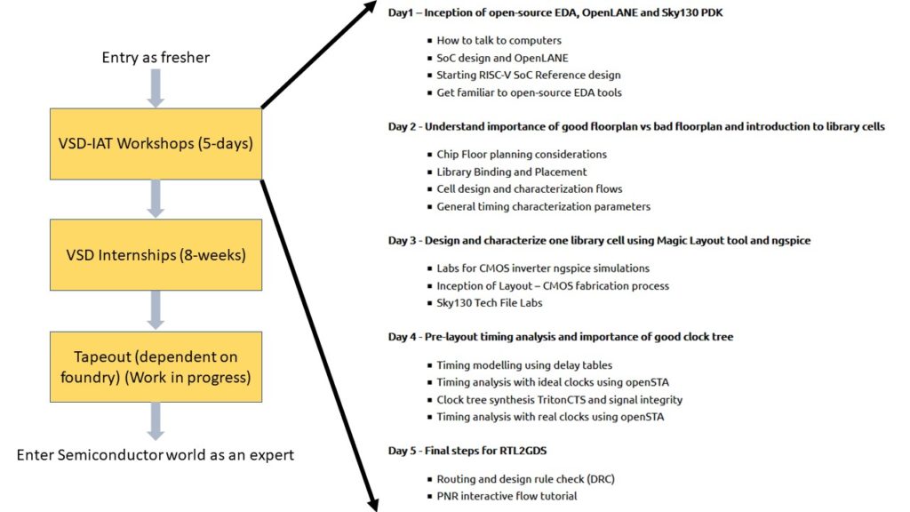
Firstly, The Training – Take a glimpse at topics. Covering from basics to advanced in 5-days, needs some real innovative and structure labs
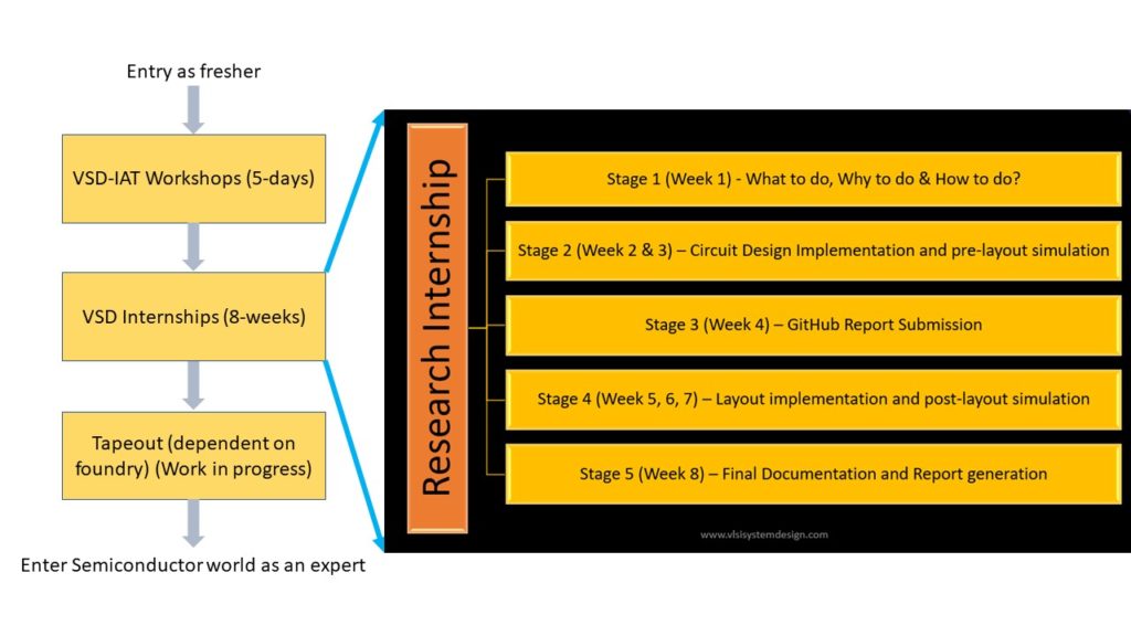
Secondly, The Internship – Take a glimpse at our VSD – 5SP (5 stage process) internship model for analog IP’s
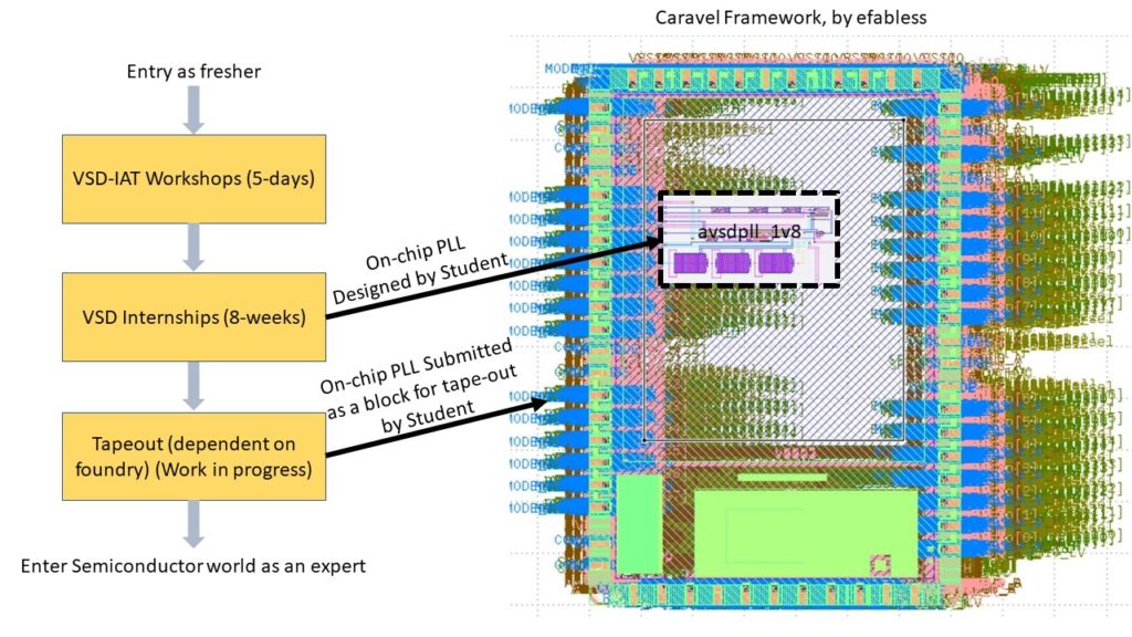
Thirdly, The Tape-out – Two months back, this was “Work in Progress”, but now, look at below image.
Most importantly – All these were done by VSD students who had no experience in VLSI when they entered VSD-IAT workshops
Can you believe what this model can do for a fresher who is looking forward to entering VLSI industry? It does not stop here, and he/she needs to continuously revise. But can you observe the VLSI training experience – A Tape-out even before his/her first job?
Looking 2 candidates – one with a tape-out experience and one without – whom will you pick?
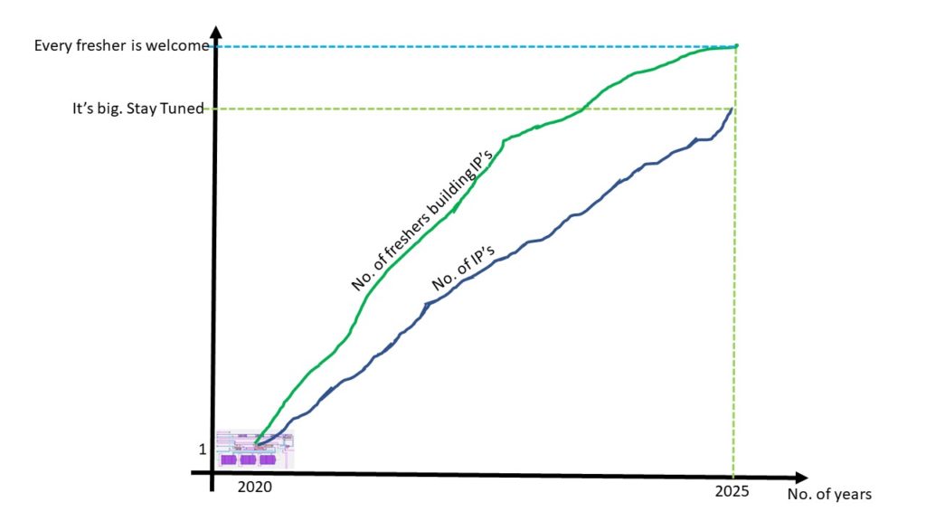
So, what next for VSD? Look at below chart, which is planned for at-least next 5 years (though we have a charter for next 15years, but would like to give you a glimpse of a short-term executable plan)
Now, the recognition-
Please join me to Congratulate Lakshmi S – MS ECE
Lakshmi had joined 5-day Workshop on VSD-IAT Physical Design and SoC design using open-source EDA tools which happened on 27th May’ 2020 and then RISC-V based MYTH workshop on 29th July’ 2020. Very soon, VSD noticed something incredibly unique within her when she submitted her pre-layout Git repo for avsdpll_1v8. It was quite evident, Lakshmi is here for the long run, and when internship finished, she was the first one with a fully completed post-layout Git repo using Skywater 130 PDK’s. Here is detailed Git repo: (GitHub is indeed the new resume)
https://github.com/lakshmi-sathi/avsdpll_1v8
Please join me to Thank Mohamed Kasseem, Tim Edwards from efabless (or as I said before, e-fabulous)
Mohamed, Tim have been in world of open-source even before I existed in this world. They were true VSD mentors from its inception and had a similar vision for open-source chips and IP’s. You will be hearing some exceptionally good news about them very soon. Without their constant push and support, I believe this would not have been realizable. They are a real bless for Semi-conductor industry
Last, but not the least, please join me to Thank Google/Skywater
As I said, this was the final piece of puzzle – opensource 130nm PDK’s. Without this, none of the above would had been possible. And VSD is grateful to Google/Skywater, due to which students now can build real silicon proven designs and IP’s
2020 has been surprising the whole world in many ways – What do you think?
Stay tuned – All the best and happy learning….
