On-Chip Variation (OCV) – Part 2

Hello

Today, I was a guest speaker at one of the biggest Technical Conference held in Bangalore, and luckily I met few people who had read my previous post. This is what I call “From Virtuality to Reality“. Its really awesome feeling, when you get to meet people personally.

We were identifying sources of variations, and below is the second one

2) Oxide Thickness

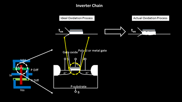
Let’s go back to the inverter layout and look which part are we talking about

Here, we are talking about gate oxide thickness variation

Below is the section from inverter chain, which we are worried about

If we go by ideal fabrication process, below is what you will achieve, a perfectly cubic shape (below is the 2D image, so it looks rectangle) oxide layer, and perfectly deposited metal gate or poly-silicon gate

But, if we go by actual oxidation process, its very difficult or almost impossible to achieve the above perfect oxide thickness. And I can confidently say that, as I have worked on fabrication for a brief period of time during my Masters at IIT Bombay.

Below is what you will actually get

So, what’s wrong having above oxide thickness. Again, its the drain current (which is a function of oxide thickness, shown in below image) that will get varied for the complete chain of inverter, especially, the one’s on the sides. The variations in middle inverters will still be uniform. We discussed the reason for this in last post

Imagine a chain of, as long as, 40 inverters or buffers ….. the variation is HUGE. And this needs to be accounted for, in STA.

So the challenge is, how to we find the range and effectively model it in STA. Are we scared ? Ofcourse Not …. 🙂

“Be thankful for each new challenge, because it will build your strength and character.”Author Unknown :),Be Thankful

Thanks

Kunal

Registration for Ethical RISC-V IoT Workshop

Welcome to Ethical RISC-V IoT Workshop

The “Ethical RISC-V IoT Workshop” at IIIT Bangalore, organized in collaboration with VSD, is a structured, educational competition aimed at exploring real-world challenges in IoT and embedded systems. Participants progress through three stages: building an application, injecting and managing faults, and enhancing application security. The event spans from May 9 to June 15, 2024, culminating in a showcase of top innovations and an award ceremony. This hands-on hackathon emphasizes learning, testing, and securing applications in a collaborative and competitive environment.

Rules :
  1. Only for Indian Student whose college is registered under VTU
  2. Only team of 2 members can Register
  3. Use only VSDSquadron Mini resources for product development
Awards :
  1. Prize money for final 10 Team
  2. 3 Winner team’s Product will be evaluated for Incubation
  3. 7 consolation prizes
  4. Completion Certificate to final round qualifier
  5. Chance to build a Proud Secured RISC-V Platform for India

Date for Registration : 9th May - 22nd May, 2024
Hackathon Inauguration : 23rd May 2024

VSDSquadron (Educational Board)

VSDSquadron, a cutting-edge development board based on the RISC-V architecture that is fully open-source. This board presents an exceptional opportunity for individuals to learn about RISC-V and VLSI chip design utilizing only open-source tools, starting from the RTL and extending all the way to the GDSII. The possibilities for learning and advancement with this technology are limitless.

Furthermore, the RISC-V chips on these boards should be open for VLSI chip design learning, allowing you to explore PNR, standard cells, and layout design. And guess what? vsdsquadron is the perfect solution for all your needs! With its comprehensive documentation and scalable labs, thousands of students can learn and grow together.

VSD HDP (Hardware Design Program) Duration-10 Week

With VSD Hardware Design Program (VSD-HDP),  you have the opportunity to push the boundaries of what exist in open source and establish the new benchmark for tomorrow.

It will leverage your degree in Electrical or Computer Engineering to work with

  • Programmable logic
  • Analog/ digital IP
  • RISC-V
  • Architecture & microprocessors
  • ASICs and SoCs on high-density digital or RF circuit cards
  • Gain hands-on knowledge during design validation and system integration.

Sounds exciting to just get started with expert mentors, doesn’t it? But we are looking for the next generation of learners, inventors, rebels, risk takers, and pioneers.

“Spend your summer working in the future !!”

Outcomes of VSD Online Research IP Design Internship Program

  1. Job opportunities in Semiconductor Industry
  2. Research work can be submitted to VLSI International journals
  3. Participate in Semiconductor International Conference with Internship Research Work
  4. Paper Publications in IEEE Conference and SIG groups
  5. Tape out opportunity and IP Royalty
  6. Interact with world class Semiconductor designer and researchers
  7. Academic professions where more research projects are encouraged.
  8. All the above research and publication work will help colleges and institutes to improve accreditation levels.

Know More Information

VSD – Intelligent Assessment Technology (VSD-IAT)

VSD – Intelligent Assessment Technology (VSD-IAT) is expertly built training platform and is suited for designer requirements. Semiconductor companies understand the value of training automation and Engineer performance enhancement, and do not need to be convinced of the impact of a virtual platform for learning. VSD trainings are quick, relevant, and easy to access from any device at any time zone.

VSD Intern Webinars

VSD Interns made it happen !!

VSD is working towards creating innovative talent pool who are ready to develop design and products for the new tech world. VSD believes in “Learning by doing principle” , and always prepare the student to apply the knowledge learned in the workshops, webinars and courses. We always push our students to work on new designs, test it and work continuously till it becomes the best performing design. Any student who enrolls to VSD community starts working with small design and grows with us and develops a tapeout level design with complete honesty and dedication towards the Work !!

Check out VSD Interns Achievement!

VSDOpen Online Conference

Welcome to the World’s only online conference in Semiconductor Industry VSDOpen Conference. With enormous support and global presence of audience from different segments of industrial lobby and academia made a highly successful event. Evolution is change in the genetic makeup of a population over time, online conference is one kind evaluation everyone adapt soon. 

  • VSDOpen 2022 is an online conference to share open-source research with the community and promote  hardware design mostly done by the student community.
  • VSDOpen 2022 is based on the theme “How to lower the cost to learn, build, and tapeout chips ?”  , which will provide a platform to community to build stronger designs and strengthen the future of Chip design.
  • VSDOpen is envisioned to create a community based revolution in semiconductor hardware technology.
  • The open source attitude is required to bring out the talent and innovation from the community who are in remote part of world and have least access to the technologies.  And now Google support will help to bring the vision to execution by VSD team

VSD Online Course by Kunal Ghosh

VSD offers online course in complete spectrum of vlsi backend flow from RTL design, synthesis and Verification, SoC planning and design, Sign-off analysis, IP Design, CAD/EDA automation and basic UNIX/IT, Introduction to latest technology – RISC-V, Machine intelligence in EDA/CAD, VLSI Interview FAQ’s.

Current Reach – As of 2021, VSD and its partners have released 41 online VLSI courses and was successfully able to teach  ~35900 Unique students around 151 countries in 47 different languages, through its unique info-graphical and technology mediated learning methods.

Enquiry Form