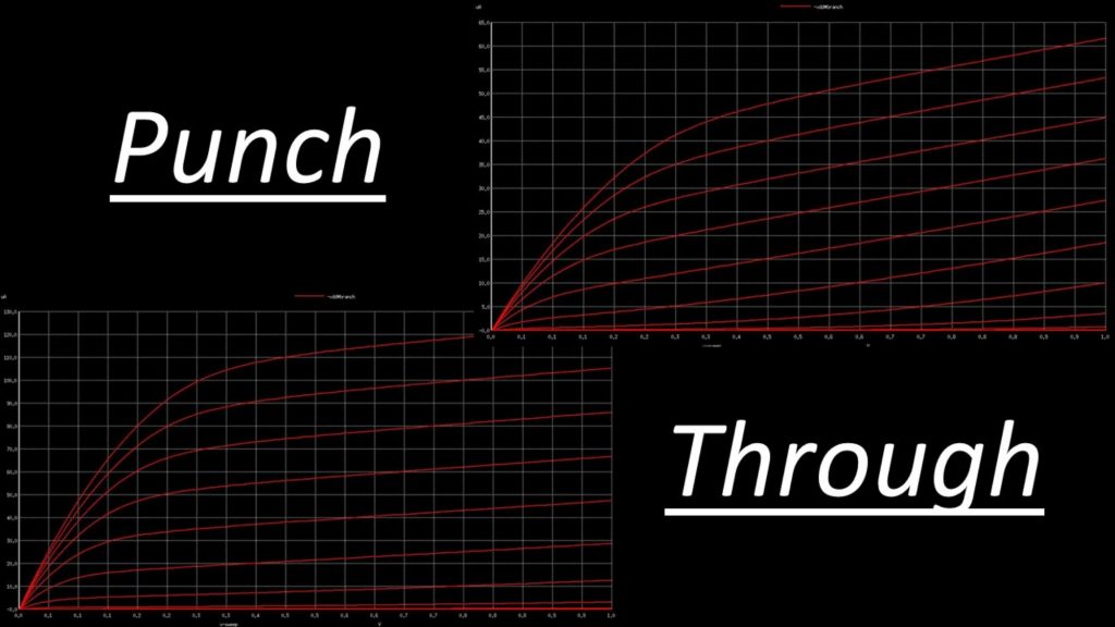
And it’s important, as this will set a back-ground for my upcoming new course on “CCS Timing Libraries”. So, in my last blog, we talked one of the effects of scaling which was ‘high interconnect impedance”. In this one, before entering details of more effects of scaling (that lead us to CCS solution), let’s view some basic Id-Vgs curves for 130nm and 32nm technology nodes CMOS inverter
Below is the image of 130nm Id-Vgs at constant values of Vds:
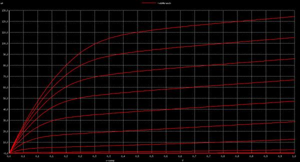
The linear or resistive nature of current with increasing Vds due to velocity saturation has been well explained in my course on “Circuit design and SPICE simulation – Part 1 and 2”. You might want to go through those courses.
Another effect which is not visible at 130nm, but very much visible in even lower nodes, like 32nm, is ‘punch-through’ effect. Look at below image which is Id-Vgs characteristics for 32nm:
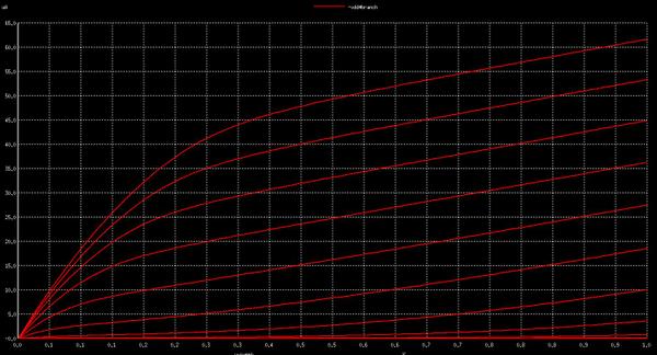
If you observe, the currents at higher voltage of x-axis, they are no more a linear function of Vds, but become a function of square(Vds).
That’s the punch-through effect. And, the concept is simple. It’s just that, when you bias your NMOS transistor, with Vd as increasing +ve voltage, Vs grounded, the drain-substrate goes reverse bias, and hence a depletion region starts to get formed near drain region at lower voltages of Vd, as shown below:
![]()
This is tricky. As Vds increases, the reverse bias near the drain region also increases.
Due to shorter channel length of 32nm, the reverse bias touches source region. Boom….. that’s when source/drain merge into a single depletion region and drain current is no longer controlled by gate. This causes a rapid increase in drain-to-source current, and which is what you see in above 32nm Id-Vgs curves.
Now as an STA engineer, that’s not my problem. My biggest problem is how do I model these complex effects of scaling in my libraries. Standard NLDM libraries just don’t help here. There are structural changes that can be done to NMOS transistor to protect punch-through effect. These extra currents has great impact on gate delays (in my next blog, I will talk about Miller effect, which again brings in extra capacitance, and hence extra currents), and modelling delays with currents are best solution to capture these effects
Find it interesting…. well….just look forward for my course on CCS timing, which will be filled with such cool and interesting concepts, and I can bet, you will not blink an eye while viewing the videos
Just like the saying goes, by Benjamin Franklin “An investment in knowledge pays the best interest”, my job is to make your investment interesting….
