Did you scale down? – high interconnect impedance – CCS timing!!

You see how every sentence in the title is connected!!!

As you are aware about the big launch on “CCS Library” course, I just wanted to bring one thing over here for you to think about. Its ‘Scaling’. We are moving from 180nm to 45nm to 7nm. Let’s take an example of 180nm and 45nm. That’s a scaling factor of 0.25 (this can be debated as 45nm/180nm will give 0.25 and vice-versa will give 4. Let’s stick to former i.e 0.25).

Now, there are tons of scaling mechanisms, like short wire, long wire, constant thickness, etc. For this discussion, let’s stick to full scaling for long wires, as shown in below image:

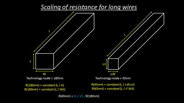
This is rather a shocking observation, and in great contrast with gate delay. Gate delay reduces year by year, whereas delay of long wires goes up by 6.25% (i.e. by a factor of sqr(0.25) = 0.0625). That’s huge!!

Let’s demo both wires in SPICE. So here we will model the wire as distributed RC network, and plot the output response V(wire_out) with step pulse as input V(out), as shown in below image. Ignore the naming convention as the course is in continuation with STA-1, STA-2, Circuit design and SPICE simulations. Do not forget to finish these courses 100% before even registering to “CCS timing” course

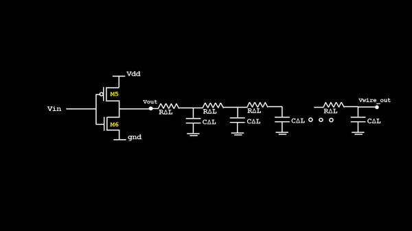
Be aware, that the problem statement here is the inverter has to drive the long wire in both technology nodes, while giving an accurate response at Vwire_out.

Assume wire length to be 50m. So, if we pluck out the wire from the above network, keep reducing the wire size by half, and just SPICE it with 180nm technology node for all wire lengths, assuming R∆L as 75K and C∆L as 100pF (taken default values from ngspice), it gives us the below response

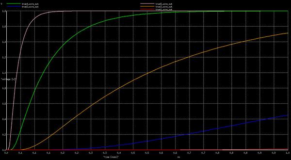
To interpret above, the bottom red line is the Vwire_out response for 50m wire, blue line is for 25m, and finally white line is for 3.125m. This can be (simply) interpreted, that, at 180nm technology node, a wire length of 3.125m can be driven by CMOS network

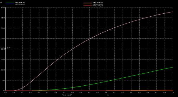
But, when we scale down in the way we shown above in first image i.e. by a factor of 0.25, we need to scale up the resistance by (1/S2) and so now the R∆L becomes (75K/sqr[0.25]) = 1200K, and let’s draw a similar step response of wire at 45nm, it looks something like below image:

Now, previous driver models for inverters i.e. thevenin or Norton model were good to express various timing arcs using output capacitance only. But they are not efficient enough to drive a high impedance network as shown above. Solution – CCS timing

Just try to solve thevenin voltage divider circuit, and you would get to know that output will just follow input voltage, which is not accurate. No issues, if you find it difficult to do so, I will be making it simpler in my course

Next step is to plot the inverter response to these high impedance network. And that’s even more interesting. Let’s keep that for next blog or for the course.

Just as Albert Einstein said “Any fool can make things bigger, more complex and more violent. It takes a touch of genius – and a lot of courage – to move in the opposite direction

Be a genius, and wait for my CCS timing course. Till then please complete 100% the necessary courses (STA-1, STA-2, Circuit design and SPICE simulations Part 1 and 2).

But please be aware of the concepts, and I will make this course a smooth and happy journey for you. Happy Learning!!

Registration for Ethical RISC-V IoT Workshop

Welcome to Ethical RISC-V IoT Workshop

The “Ethical RISC-V IoT Workshop” at IIIT Bangalore, organized in collaboration with VSD, is a structured, educational competition aimed at exploring real-world challenges in IoT and embedded systems. Participants progress through three stages: building an application, injecting and managing faults, and enhancing application security. The event spans from May 9 to June 15, 2024, culminating in a showcase of top innovations and an award ceremony. This hands-on hackathon emphasizes learning, testing, and securing applications in a collaborative and competitive environment.

Rules :
  1. Only for Indian Student whose college is registered under VTU
  2. Only team of 2 members can Register
  3. Use only VSDSquadron Mini resources for product development
Awards :
  1. Prize money for final 10 Team
  2. 3 Winner team’s Product will be evaluated for Incubation
  3. 7 consolation prizes
  4. Completion Certificate to final round qualifier
  5. Chance to build a Proud Secured RISC-V Platform for India

Date for Registration : 9th May - 22nd May, 2024
Hackathon Inauguration : 23rd May 2024

VSDSquadron (Educational Board)

VSDSquadron, a cutting-edge development board based on the RISC-V architecture that is fully open-source. This board presents an exceptional opportunity for individuals to learn about RISC-V and VLSI chip design utilizing only open-source tools, starting from the RTL and extending all the way to the GDSII. The possibilities for learning and advancement with this technology are limitless.

Furthermore, the RISC-V chips on these boards should be open for VLSI chip design learning, allowing you to explore PNR, standard cells, and layout design. And guess what? vsdsquadron is the perfect solution for all your needs! With its comprehensive documentation and scalable labs, thousands of students can learn and grow together.

VSD HDP (Hardware Design Program) Duration-10 Week

With VSD Hardware Design Program (VSD-HDP),  you have the opportunity to push the boundaries of what exist in open source and establish the new benchmark for tomorrow.

It will leverage your degree in Electrical or Computer Engineering to work with

  • Programmable logic
  • Analog/ digital IP
  • RISC-V
  • Architecture & microprocessors
  • ASICs and SoCs on high-density digital or RF circuit cards
  • Gain hands-on knowledge during design validation and system integration.

Sounds exciting to just get started with expert mentors, doesn’t it? But we are looking for the next generation of learners, inventors, rebels, risk takers, and pioneers.

“Spend your summer working in the future !!”

Outcomes of VSD Online Research IP Design Internship Program

  1. Job opportunities in Semiconductor Industry
  2. Research work can be submitted to VLSI International journals
  3. Participate in Semiconductor International Conference with Internship Research Work
  4. Paper Publications in IEEE Conference and SIG groups
  5. Tape out opportunity and IP Royalty
  6. Interact with world class Semiconductor designer and researchers
  7. Academic professions where more research projects are encouraged.
  8. All the above research and publication work will help colleges and institutes to improve accreditation levels.

Know More Information

VSD – Intelligent Assessment Technology (VSD-IAT)

VSD – Intelligent Assessment Technology (VSD-IAT) is expertly built training platform and is suited for designer requirements. Semiconductor companies understand the value of training automation and Engineer performance enhancement, and do not need to be convinced of the impact of a virtual platform for learning. VSD trainings are quick, relevant, and easy to access from any device at any time zone.

VSD Intern Webinars

VSD Interns made it happen !!

VSD is working towards creating innovative talent pool who are ready to develop design and products for the new tech world. VSD believes in “Learning by doing principle” , and always prepare the student to apply the knowledge learned in the workshops, webinars and courses. We always push our students to work on new designs, test it and work continuously till it becomes the best performing design. Any student who enrolls to VSD community starts working with small design and grows with us and develops a tapeout level design with complete honesty and dedication towards the Work !!

Check out VSD Interns Achievement!

VSDOpen Online Conference

Welcome to the World’s only online conference in Semiconductor Industry VSDOpen Conference. With enormous support and global presence of audience from different segments of industrial lobby and academia made a highly successful event. Evolution is change in the genetic makeup of a population over time, online conference is one kind evaluation everyone adapt soon. 

  • VSDOpen 2022 is an online conference to share open-source research with the community and promote  hardware design mostly done by the student community.
  • VSDOpen 2022 is based on the theme “How to lower the cost to learn, build, and tapeout chips ?”  , which will provide a platform to community to build stronger designs and strengthen the future of Chip design.
  • VSDOpen is envisioned to create a community based revolution in semiconductor hardware technology.
  • The open source attitude is required to bring out the talent and innovation from the community who are in remote part of world and have least access to the technologies.  And now Google support will help to bring the vision to execution by VSD team

VSD Online Course by Kunal Ghosh

VSD offers online course in complete spectrum of vlsi backend flow from RTL design, synthesis and Verification, SoC planning and design, Sign-off analysis, IP Design, CAD/EDA automation and basic UNIX/IT, Introduction to latest technology – RISC-V, Machine intelligence in EDA/CAD, VLSI Interview FAQ’s.

Current Reach – As of 2021, VSD and its partners have released 41 online VLSI courses and was successfully able to teach  ~35900 Unique students around 151 countries in 47 different languages, through its unique info-graphical and technology mediated learning methods.

Enquiry Form