
A few months back, I came across a workshop titled ‘RISC-V based Microprocessor for You in Thirty Hours (MYTH)’, that was about designing RISC-V core using TL-Verilog organized by Steve Hoover and Kunal Ghosh in just 5 days!! Talking about designing processors has always made me excited to work with. So, I participated in the workshop and was highly appreciated by the content as well as the support given by the team.
Now, I would walk through the content of the workshop and how I successfully completed it in 5 days! Day 1 is brief of RISC-V ISA and its software tool-chain. From Day 3 on wards, it is RTL implementation of RISC-V core which has the support of RV32I Instruction format. Day2 talks about the Application Binary Interface (ABI) which is the bridge between software (application program) and hardware (registers specific to the architecture of system).
Now, going into more technicality I would like to compare the workshop flow with standard VLSI front-end design flow.
Step 1: Specification – Any design/logic we write in any language, cannot be written without its specification
- Base Integer RV32I containing 47 unique instructions
- 6 types of Instructions – R, I, S, B, U, J
- Number of integer registers are 32 and width of these registers is 32, hence refers to 32-bit address space
More details on RISC-V ISA can be obtained here.
Step 2: High-Level Design
- Compiled C code on RISC-V ISA using RISC-V GNU Toolchain
- `objdump` – to view assembly code
- RISC-V ISA Spike Simulator – to run the C code
- Spike as debugger – to check internals of RISC-V registers
Before going to Step 3, I would like to give a brief about ABI. It is a set of rules enforced by the Operating System on a specific architecture. So, a relocatable machine code is converted to absolute machine code via an ABI interface specific to the architecture of the machine.
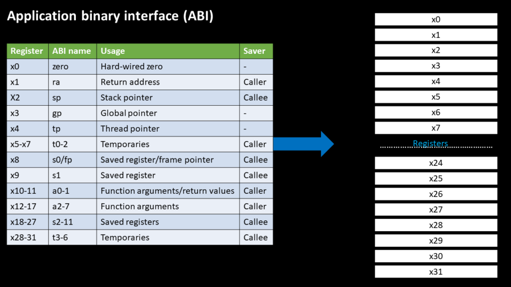
Image Source: https://riscv.org/wp-content/uploads/2015/01/riscv-calling.pdf
Now, to get familiar with TL-Verilog, we have used Makerchip, a free online environment for developing high-quality integrated circuits, as the platform through which you can code, compile, simulate and debug Verilog designs, all from your browser in a single tab!
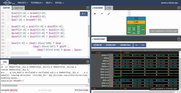
Example: Combinational Calculator
To check more tutorials and features about TL-Verilog check here under the Tutorials section.
Step 3: Low Level Design
- RISC-V basic microarchitecture design i.e. Fetch-Decode-Execute
- Started to design individual building blocks in TL-Verilog on Makerchip IDE
Step 4: RTL Coding
- Connected all building blocks with starter code containing Register File, Instruction Memory, and Data Memory as a black box
- Completed 5-stage pipelined RISC-V processor
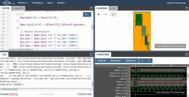
RISC-V 5 stage pipelined processor
Step 5: Verification
- In general, Makerchip uses LFSR based random generator for inputs to verify the design.
- Now, specific to RISC-V core we have given a test case (i.e Summation of 1 to 9)which is dumped into Instruction Memory.
- You can observe summation of 1 to 9 (i.e. 45) is stored in r10 in Register File.
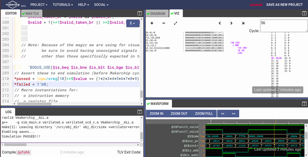
Test Case: Output
Key Takeaways:
- TL-Verilog – Simple, Powerful, and Flexible
- Open-Source RISC-V – denoted as the Linux of hardware
- Application Binary Interface – bridge between software and hardware
Future work:
- FPGA Implementation of MYTH core
- SoC design for testing RISC-V IP
Author:
Shivani Shah is currently a research student at the International Institute of Information Technology (IIITB), Bangalore. She was a participant in RISC-V MYTH Workshop by VSD and Redwood EDA in the second iteration. From the third iteration onwards, she is TA for this workshop.
In-depth documentation about this workshop can be found here: https://github.com/shivanishah269/risc-v-core.
![]()
