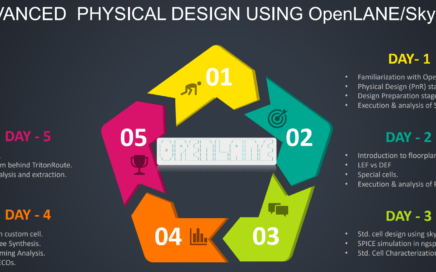
Ever heard of Chip Design Pentagon?

Know what Pentagon is? It is a plane figure which has 5-straight sides and 5-angles. For a perfect pentagon, it needs all its sides and angles to be the same, till the last decimal. Do you know what is the similarity between pentagon and our upcoming workshop “Advanced Physical Design workshop using OpenLANE/SKY130”?  Look above image and you would guess it right. It is a perfect blend of topics where even a fresher can jump-start his/her career in chip design in just 5-days

Continue reading

2nd mile-stone in field open-source (open-lane EDA + Google/Sky130)

@Nickson joined our research project group under VSD Research internship program which runs for 8-weeks. He was supposed to develop flow for standard cell design and characterization using all open-source tools – magic/ngspice, then plug those standard cells into open-source PNR flow by open-lane, and benchmark RTL2GDS flow results. This needed a knowledge, not only of PNR, but device physics, custom layout, DRC/LVS and then (finally) Physical design/STA.

Continue reading

The horrible std cell ever designed by me….

Power rail discontinuity – We would like to have continuous power rail.N- and P-diffusion discontinuity – We would like to have continuous diffusion. For my Physical design friends, remember, we add “FILLER” cells at the end of routing, and you always wondered why we are doing so.Small substrate contacts – Except for inverter, all substrate contacts are single width, which will create high resistance path for current, thus increasing “Clk-to-Q” delay.Hanging metal1 – If you see for the NAND gate outputs, there is lot of hanging metal1.

Continue reading