“Research is to see what everybody else has seen, and to think what nobody else has thought” – Let’s prove this by end of this blog
Hi Everyone
In the series of FAQ’s, here is the next one – an important one. Now, once you have made a layout, next step is to extract SPICE netlist, provide the right stimulus and analyze. There are good commands and techniques inside MAGIC to do this for 180nm process node (very good for learning VLSI concepts, refer to this course to learn more about MAGIC layout techniques at 180nm technology node)
Now to enable this, there was a series of questions I had prepared back then in 2014, when I was making this online course for students looking for VLSI jobs in layout, I would like to share those, some of you might be benefit by this. This was done with Tim Edwards – SVP Analog, Efabless Corp. Pvt. Ltd.
Question) Hi Tim,
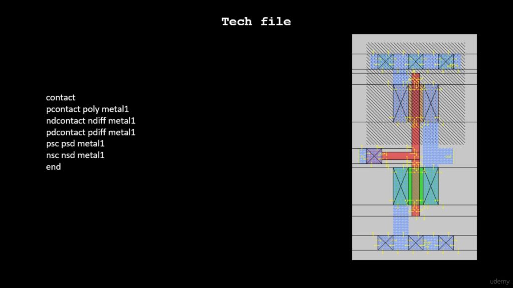
I am using the attached min.tech file and trying to do ext and ext2spice. I read in your manual, that we need to have ‘connect’ section defined clearly to extract the connectivity information, which I did. Still for some reasons, it’s not extracting the SPICE netlist (i will look into the capacitance and resistance extraction later). Is there anything else I need to add in tech file (please ignore the DRC section in tech file for now. I need to update it yet)
Attachments – min.tech and INV.mag (for attachments, please refer to this course)
Answer) Except for some parasitics, magic won’t extract much if there isn’t at least one active device, so you’ll need a device extraction statement.
Try
device mosfet pmos pfet pdiff,pdc nwell Vdd!
device mosfet nmos nfet ndiff,ndc pwell Gnd!
However, I would like you to start using the “substrate” command for extract, which allows you to specify “space/well” as “substrate”, and this will properly extract the substrate and follow the substrate
tap connectivity. Your annotated files are attached, with the techfile renamed to “min2″ from “min”. “INV.mag” is the same, but I have changed the technology name to “min2” from “scmos” (I don’t like the practice of naming everything “scmos”, because it makes it very hard to keep track of the technology used for a particular layout). I will add some other things that I think are important but do not show up in the traditional SCMOS techfiles, such as extract and DRC “style” sections, the “stackable”
keyword for the contacts section (although none of your contacts is stackable, in this simple techfile).
Question) Thanks a lot Tim. Sure, I will wait for your updated tech file.
Answer) Here is a “basic” techfile I made once that supports a basic CMOS process (no special devices like bipolars or high-voltage or thick-oxide, although it does have varactors) with 6 metal layers. The
scalefactor corresponds to a 0.18um process.
The techfile style is pretty up-to-date, with DRC and extract sections that use values in microns, wide spacing and exact-overlap rules in the DRC, use of “copyup” in the cifinput section, a LEF input section, stackable contacts, substrate extraction, layer name aliases, named styles, 3D rendering, simplified parasitic description, and the updated extraction devices. That’s a comprehensive list of everything I’ve added to the techfile format in the past 20 years or so.
Question) Thanks a lot Tim. I think for the INV.mag which I am using, I can skip metal1+ layers info, right? That will make the tech file even short and simple
Answer) Yes, of course. I just gave you the file that I had, without much editing, but of course you can simplify it further by removing everything above metal1.
So, a lot of research went behind making of this online course. Here’s the link for the same-
https://www.udemy.com/vlsi-academy-custom-layout/
All the best and happy learning
