
Hello
In my last blog, which received huge response, I talked a simple and efficient technique for clock gating. But it came with an additional cost of an extra clock gating setup and hold check. And the reason for those checks was, mainly, to get rid of unacceptable glitches in the EN pin.
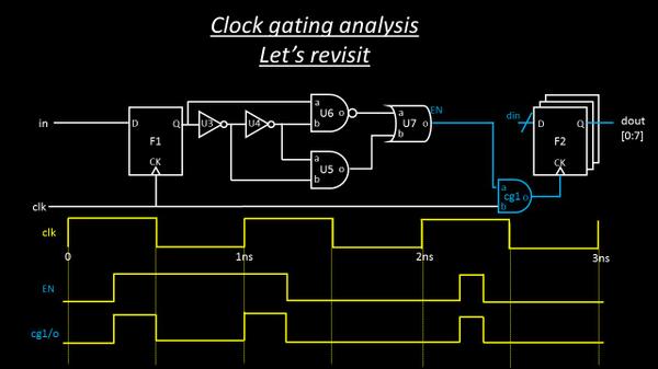
What if, we do some more changes to the clock gating circuit and make it more efficient to detect and eliminate glitches, without even having an additional clock gating setup and hold check exclusively. How about having these checks inherently in the circuit? Let’s talk about it a more. Before that, have a look at below image and the waveforms at EN pin, because of which we had to add additional checks
Now let’s add a level sensitive latch in between U7 and cg1, and now re-look at the waveforms again, in below image
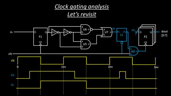
So whenever, clock is low, the latch will be transparent, and EN which is high from 0.5ns to 1ns will get latched at the output of L1, and will remain high until there is a change in EN signal till next clock edge (note the latch clock is inverted, so will be transparent in low level of clock signal)
Now when the next clock low level arrives at latch clock pin between 1ns to 1.5ns, the EN signal goes high to low, and by the end of 1.5ns, the EN is low, which now gets latched at the output of L1
When the next clock low signal arrives between 2ns to 2.5ns, the EN goes high momentarily and then goes low, and by the end of 2.5ns, the EN goes completely low. So the glitch gets removed by the end of clock cycle. Isn’t that a solid technique to get rid of glitches on EN pin? Looks great, but latches have their own set of problems (will talk about it more in following posts).
But with that circuitry, if you go ahead and analyze the output of cg1:o, it will match with what we expected or have seen in past clock gating blog as shown below
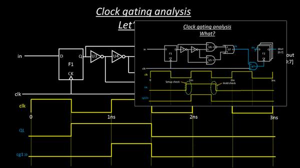
Also, I would leave it to your imagination as in what happens when the glitch arrives somewhere at edge of clock low-to-high and high-to-low i.e. for eg, somewhere at 1ns or 1.5ns or 2ns.
It would be easy to analyze if you go by the above timing graph method.
There is another problem with above latch based clock gating. The wire between latch output and AND gate input needs to be carefully routed, else it would result in weird violations.
But you know, that’s also been resolved. You just need to find out how, in my STA-2 course.
The initial reviews has been real great. One reviewer says the below:
“I understand now why STA II was delayed. Kunal has taken great efforts to get Hands ON training with Opentimer tool. Gets some getting used to but Kunal makes it easier for me video after video. Had enjoyed enjoyed STA I and now looking forward to get STA II completed soon.”
So get in and find similar answers and cool techniques to all your timing problems.
Till then….
happy learning !!!
