Hello
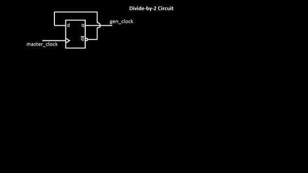
I get this one occasionally … not particularly about the concept, but about the ways we can create a generated clock definition. Too many options make it too complex… But you know what, with a handful of images, this topic becomes way too simple… Let me show how? Start with below simple divide-by-2 circuit and try to define it in all ways possible
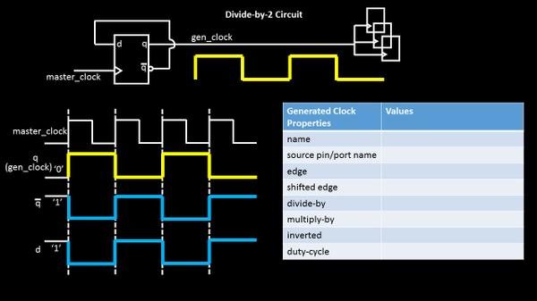
I believe, best way to understand any topic is the ‘graphical way’. So, let me show you how the input and output wave-forms look like, in below image
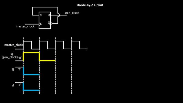
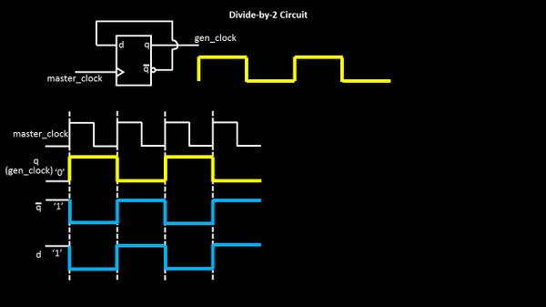
If you start with master clock of say 1ns period, the output is expected of 2ns period (frequency divide-by-2). So at the first rising edge of clock (assuming the initial state of circuit is ‘q’ = 0 and ‘d’ = 1), the data at ‘d’ pin will be propagated at ‘q’ output (since it’s a rise-edge triggered flop), and ‘q’ becomes ‘1’, ‘q_bar’ becomes ‘0’, and ‘d’ is at ‘0’ (‘q_bar’ is connected to ‘d’). This is shown in above image. While, we keep doing this, the state of the circuit changes at every rise edge of master_clock, and below is what you get
Now that was the digital hardware part of it. Let me tell you a secret of ‘static timing analysis’ of ASIC…We are ‘static’. We need definitions. We understand software language. And we will not change J . You are right in thinking.. We are adamant on this J
Designer – Ok, so let me speak to you in your language. Let me write a define this new ‘gen_clock’ for you so you understand it and use it
STA – you better do !!
Seriously, I have worked ~6 years in this area, and believe me, these analysis is very rude 😉
Anyways, coming back, we need to fill up below table so that the analysis engine understands it and passes this information to further flops clock pins, it might be driving
By the look of it, below seems to be most appropriate and valid values for ‘gen_clock’

Though this looks the easiest, there are other ways to define this (not recommended for this simple one). So if we were to define the gen_clock based on the edges of master clock, below how it will like. We remove the ‘divide-by’ option and use the edge values of 1,3,5 to define the new clock. This says, that at ‘1’ edge of master_clock, the first rise edge of gen_clock arrives. At ‘2’ edge of master_clock, the first fall edge of gen_clock arrives, and at ‘3’ edge of ‘master_clock’, the second rise edge arrives.
Isn’t that simple…wait a sec, it was simple because I took a simple example. Let me come up with a more complex circuit, break it down to little pieces and explain how to fill up this table
As H.L.Mencken said, ‘For every complex problem, there is an answer that is clear and simple’
Let’s stick to it and solve larger problems ….
Happy Learning.