I started as Physical Design Engineer, moved to STA lead and stayed there for some time. While I did love my job, I always wanted to explore and learn more, and so within a year of my last job, I learnt and moved towards library characterization (Thanks to Rohit from Paripath), RISC-V processor (Thanks to SiFive and Prof. David Patterson) and frontend TL-verilog domain (Thanks to Steve Hoover from Redwood EDA)
While I learnt and mastered these topics, I did offer them as a course for everyone to master it, directly from experts mentioned above. And now I see lot of people like me upgrading their skills, just like I did. If you are a follower of my blogs/post, you must have seen certificates that people of other domains have achieved. This shows that they did complete assignments, learnt something new and upgraded
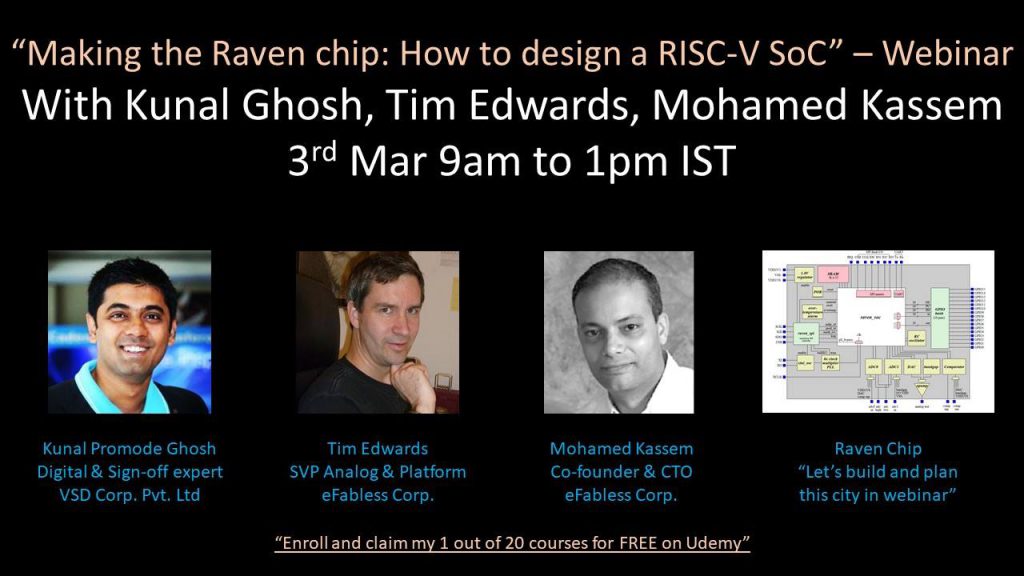
With that said, I and my company still want to explore and master more topics, which led us to partner and conduct the next webinar happening on 3rd March with Tim Edwards and Mohamed Kassem. This webinar moves us from VLSI to System Design space (hence the company name VLSI System Design [VSD]). Here’s the link. For the first time, this is an online webinar with real 180nm process from XFAB
http://go.eventshigh.com/h4p1q
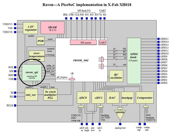
To plan and design SoC, you need to choose the right components and make sure all components work together seamlessly. Let’s start with a very important component of SoC – SPI (serial peripheral interface). Highlighted in above image. The choice of SPI varies from design to design, let’s talk a little bit about general SPI concepts first, while Tim will talk about choice of SPI in an application, in webinar
These are meant to be bus structures for data, whose characteristics distance is may be less than 10cm. These are short interconnect buses. They are not meant to be a substitute for internet
SPI – Advantage
- Full duplex
- Pretty fast: roughly bit rate half the clock rate. We can do 8Mbit bit rate on 16Mhz CPU
- 3 wires
- Addressed by chip select
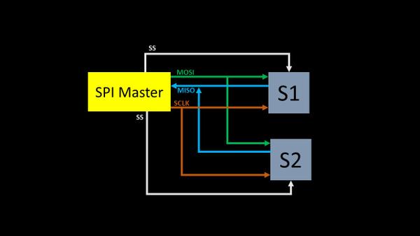
SPI model is a master/slave model. There’s some SPI master which determines who gets to transmit and who gets to receive. The output from SPI master is called MOSI (Master Out Slave In). If you have 2 slaves, slave 1 and slave 2, as shown below, MOSI goes to all the slaves
Then you have another line MISO (Master In Slave Out). All the wires are connected, as shown in below image. Then you have a master only function called SCLK, which goes to all the slaves. Now also, there must be a slave select (SS) for S1 and a slave select for S2.
The physical construction is quite easy, just tie all the data in lines on the slaves to MOSI and all data out lines MISO. And all SCLK’s get tied to the master. One of the most annoying things about SPI is that every single manufacturer of any SPI device has different names for these pins (check out raven_spi in webinar)
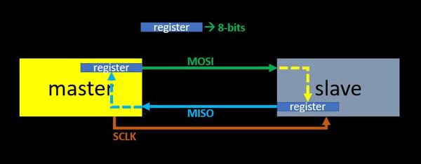
SPI transfer protocol is 8-bit usually synchronous and master generates clk. The master always initiates the transfer by asking to transmit. So, the master always transmits, and a byte always comes back from the address of the selected slave at the same time. When the master loads a byte into the SPI transmit register, the hardware starts clocking the bit out of slave and simultaneously clocks bits from slave to master. In 1-byte time, which can be as little as a microsecond at 8MHz clock rate, you get a result back. Note: If you are running the clock that fast, there is very little reason to ever use a SPI interrupt, because you can’t get in and out of an interrupt in 1 microsecond
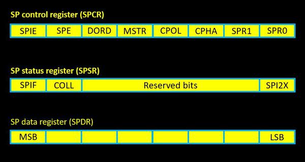
The 3 registers that control SPI:
- SP control register (SPCR)
- SPIE bit (Serial Peripheral Interrupt Enable) – If you are running full speed again, you wouldn’t do the interrupt enable. If you’re running at low speed, you’d want to have the system signal you when the transfer is done
- SP Enable bit – Unless you turn that on, SPI is not going to work at all.
- Data order bit (DORD) – with msb first is ‘0’, LSB first ‘1’
- MSTR (master slave bit)
- 2 very cryptic bits CPOL (clock polarity) and CPHA (clock phase)
- SPR1 and SPR0 – Rate 1 and Rate 0
Clock polarity is an informative system about whether the peripheral likes to have its data, true on clock high OR true on clock low. And the phase is some measure about whether it should be valid on the edge or valid on the hold. And again, every single different manufacturer of SPI devices uses different terminology for the clock phase and clock polarity and the only way you will be able to figure out to make it work is to try all four
- SP status register (SPSR)
- SPIF bit (Serial peripheral interface flag) – Don’t touch that
- Data collision flag – if you decide to write, if for some reason due to code error, you decide to write into the transmit register before the transmit is finished, before the last transmitter is finished, you will get a collision error
- SPI2X bit – speed bit. That’s a double speed bit
- SP data register (SPDR)
- The only manipulation you can do on this is, to write or read from it, you write to it, you start an SPI transfer, if you read from it, you read from it.
Now as I said earlier, the choice of SPI varies from design to design, we need to look into how to choose SPI for a particular application, in our webinar, it’s a Raven SoC.
Do you want to look the big picture? Do you want to know, where and how are your physical design skills being used? Do you want to know how to STA SPI? Do you want to know how to RTL a SoC? If you look at it, we all are a small part of the big SoC, and we are all doing our part very well. Its time, for me and you to investigate the bigger picture of SoC and start doing our jobs in collaboration to SoC planner. All these will be answered in upcoming webinar on 3rd March with Tim Edwards and Mohamed Kaseem.
Below are the webinar details. I will see you on 3rd March for another exciting 4 hours. Till then, happy learning…
http://go.eventshigh.com/h4p1q