Hello
Long time … since my last post …. Reason : Hopefully, I have given enough time for you to get hold on my previous 3 posts. Now, that you have gone through the previous one’s, this one will be easy to relate. Let’s start
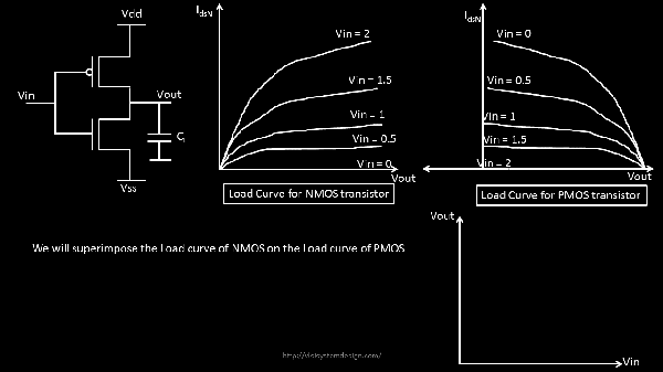
Step 3: Lets superimpose the below curves on each other (will tell you very soon, why I am doing so), and mark the x-y axis with 0V to 2V (as that’s the highest voltage we are analyzing this circuit for)

Step 4: Now, if you carefully look into the super-imposed curve and pick up the first intersection point of Vin(PMOS) and Vin(NMOS), you will find that at Vin = 0V, the Vout = 2V and …. (sentence continued after below image)

…..(sentence continued from above) and at that point, PMOS is in linear region and NMOS is cut-off. So, let’s plot that point on the below CMOS x-y axis

Similarly, (next intersection), when Vin = 0.5V, Vout = 1.5V to 2V

If I keep doing this for all intersection points, below is what I get

Tadaaaa …… and there is the CMOS VTC curve ....
Doesn’t this curve look familiar… And don’t you use this, almost, daily in all your timing analysis run ? Next, is to relate this curve to delay of cell…. I will start a separate thread for that
Now that you know, from scratch, what’s that is driving the delay of cells, I am sure you would look your Timing analysis from a different angle.
“Learning is about seeing things from a different perspective. My role is to help people improve their vision“ – Bob Selden
Kunal
