Hello
Now “black box” is what I am trying to open up for you. Let’s continue
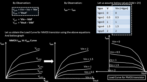
The below is called the load curve of PMOS and its a function of only Vin and Vout (no internal voltages anymore)
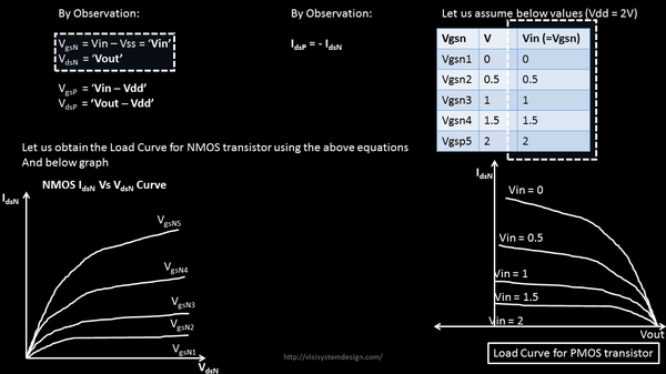
Step 2:In this step, we would take the above NMOS Ids-Vds curves, and convert them as a function of ‘Vin’ and ‘Vout’. We would use a similar approach, take the equations on top left box, and plot.
For NMOS, things are pretty simple, as the NMOS is present at bottom of CMOS inverter, and hence, it’s as good as analyzing NMOS as an independent transistor.
For eg. ‘Vgsn’ becomes ‘Vin’ and ‘Vdsn’ becomes ‘Vout’. Its just a matter of replacing the above voltage names and there you go !!
So, now that you have the load curves for both transistors, it’s just a matter of just connecting the below 3 objects
1) Load curve for PMOS transistor
2) Load curve for NMOS transistor
3) CMOS inverter
![]()
“Creativity is just connecting things“ – Steve Jobs
Lets do that in my next post 🙂
Kunal
