Hello
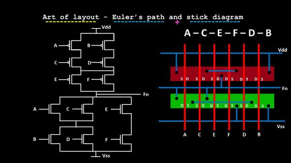
I wrote about euler’s path and stick diagram in two different blogs, but now is the time to show you how are they connected.
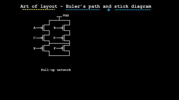
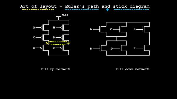
It’s simple and, seems, they can’t be separated out from each other. To prove that, let’s take a random logic using the below pull-up network…… (sentence continued after below image)
……(sentence continued from above image) ….. and let’s use the CMOS duality theorem to build the equivalent pull-down network (I will talk more about duality theorem in my courses). For now, let’s argue about this: Using de-morgan’s theorem, it can be shown that parallel connections of transistors in pull-up network corresponds to a series connection of pull-down networks and vice-versa i.e. dual networks
Based on that, below is the equivalent pull down network:
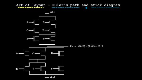
and here’s the whole circuit, with its respective funtion Fn :
The first rule of any layout : Its characteristics in pre-layout phase should match with the characteristics of post-layout phase. Barring few parasitics delay, the shape and nature of waveform should exactly match. Considering that, I did a pre-layout SPICE simulation of the above network and below is what I get: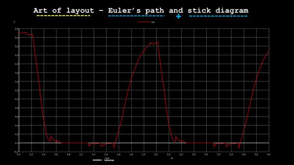
If , till this part, is clear and concise, the next job is to simply use the concepts of euler’s path and stick diagram, implement the layout and simulate it to get the above waveform….easy….right?
“All truths are easy to understand once they are discovered; the point is to discover them“ – Galileo
For freshers, doesn’t this look as a discovery….Wait n watch….there’s more….
In the meantime, you can find all such cool discoveries in my courses. Below is the link to all of them…..happy learning ….
