Hello
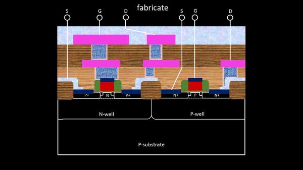
If you look into the above image, and wondering how complex it is to build and package a chip, you will change your opinion after the 16-masks that I would show in this and following blogs
Note: The 16 mask process is also covered in detail in my new course, for which the link is below:
https://www.udemy.com/vlsi-academy-custom-layout
Let’s skip some process steps and look into 1st mask below:
![]()
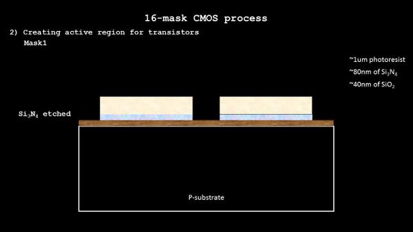
This is to create the active regions to build pmos/nmos transistors…will be evident as we move forward.
So the mask is actually an opaque plate which blocks the UV light to react with certain areas of photo-resist. As shown above, part of resist is exposed to UV light, which gets washed away giving us the below open areas for further process steps, to etch away Si3N4:
Active regions are isolated from each other using isolation SiO2 (shown in below image), which is grown with ‘LOCOS’ technique (Local Oxidation Of Silicon).
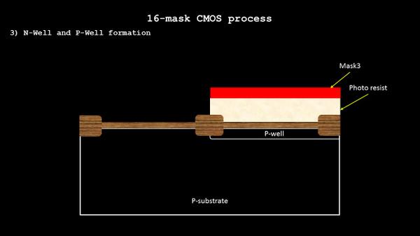
Mask2 and Mask3 will be used to create wells (nwell for pmos and pwell for nmos) as shown in below images:
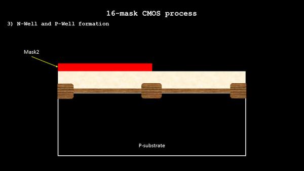
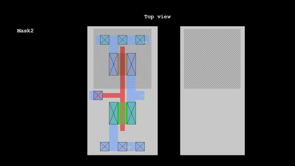
Now, if you want to actually relate a mask with layout, below image explains it all. Mask2 is nothing but the shaded nwell mask in a layout term
There are certain exchange of files that goes on between foundary and designers as a means of communicating design and process information. I will get back to this soon
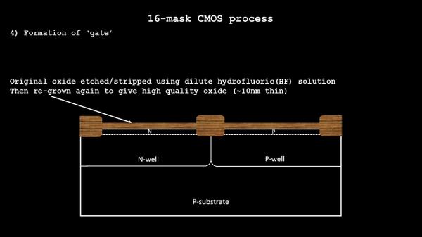
Mask4 onwards is one where we create the most critical terminal of MOSFET i.e. gate terminal. So stay tuned with me and I will take you through an exciting journey of 16-mask process, and the process will never so complex as you thought….
Happy Learning !!!
