My name is Ashutosh Sharma. I wanted to share the learnings of my eight weeks summer internship in 2020 at VSD Corporation. So, here is my journey of thoughts and processes which happened with and within me. I hope you find it insightful.
I worked as an Analog IP Design Intern at VSD Corporation. The experience which I got under Sir Kunal Ghosh was very delightful. During the eight weeks, I practiced the process of doing research extensively. After performing it, I became more confident to work out any given research problem statement.
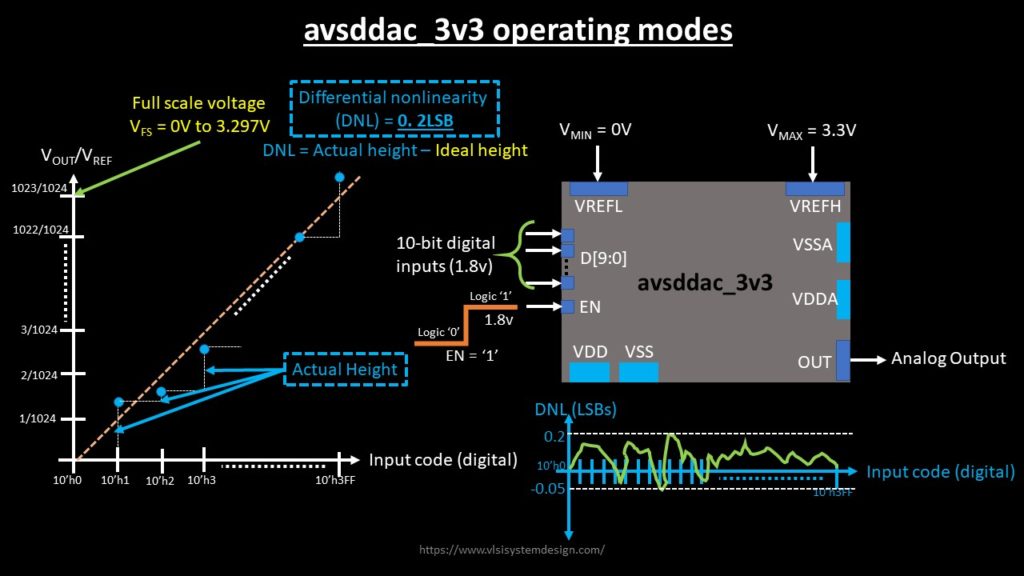
This research internship program was for eight weeks with a sequential six-staged format. My assigned objective was to design a 10-Bit Digital to Analog Converter using osu180nm tech node and open-source EDA tools.
The specs were on the VSD corporation website. The first week’s task was to research the given topic. So, I read about the given topic through various sources. I got some idea and then thought of reading the three chapters related to ADC and DACs from CMOS: Circuit Design, Layout, and Simulation, a book by R. Jacob Baker. By this, I got to know many things associated with DACs.
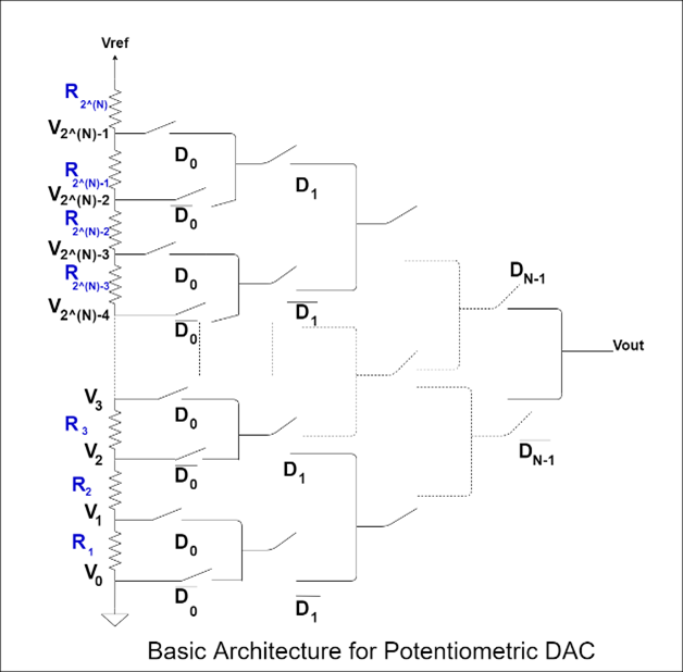
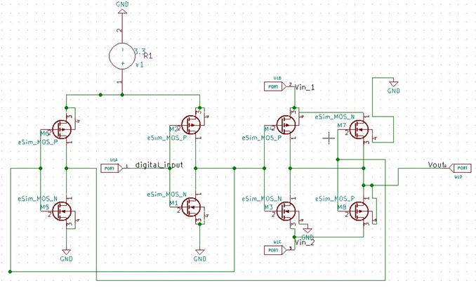
The basic idea, which I understood in DAC is to divide the voltage into N different voltage values in the range of Vref+ and Vref- for an N-Bit DAC. The design I used to achieve this is the simple resistor string DAC which consists of resistors in series. These resistors are then connected to various switches in such a fashion that it routes the exact voltage to the output.
Have a look at the simplified architecture for potentiometric-DAC given below.
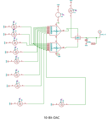
I reduced the problem of the largeness of the circuit by building hierarchical subcircuits of switch, 2 Bit, 3 Bit, 4 Bit,…..till, 9 Bit DAC, and then used two 9 Bit DAC to build the 10-Bit potentiometric DAC.
Given below is the block diagram of the DAC –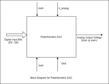
Using the gathered knowledge, I wrote a 3-page article to submit to go to stage 2.
The stage-2 task was to make the layout of the circuit using eSim and simulate it using ngSpice.
So, using the hierarchical design I completed the circuit of 10-Bit all the subcircuits including switch, 2 Bit, 3 Bit, 4 Bit, ….., 9 Bit DAC.
 |  |  |  |
| |  |  |  |
I had two weeks to show the pre-layout simulations. I finished the schematic part in time.
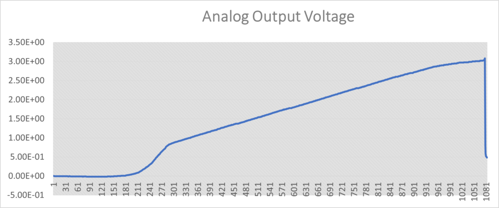
But the output values of Vout v/s Digital Values were very much irregular, especially at the starting of it.
I had no courage to calculate the INL and DNL values for them. Because what happens is that even a slight deviation in the Vout v/s Digital Values graph gives you an avalanche in the error value graph.
I found that the problem was inside the switch that I had built using only four transistors.
I cured this problem by designing a better one, resizing the nmos and pmos transistors, and tweaking the capacitor between V_out and gnd.
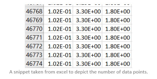
Another problem that I faced was in the calculation of the errors. The simulator gives an enormous number of data points.
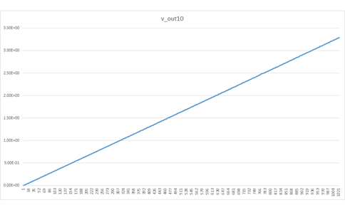
So, I used my programming skills to automate that task of redundant computations and got results quickly. The following shown is the graph of analog output voltage versus input digital values.
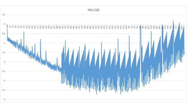
The next shown is the INL(LSB) v/s Digital Code Graph for 10-Bit DAC.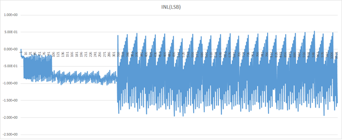
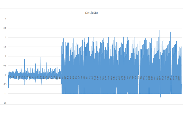
The next shown is the DNL(LSB) v/s Digital Code Graph for 10-Bit DAC.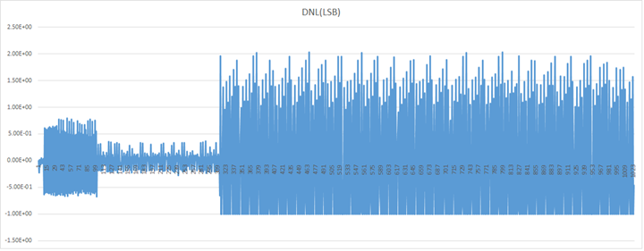
The next and a bit easy part was to upload these findings on GitHub, which is xzlashutosh/avsddac_3v3: This repository contains the design and simulation process and results of potentiometric digital to analog converter. (github.com)
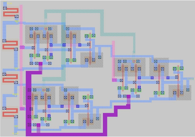
The seventh week was to complete the layout of the circuit. Tackling some more challenges such as – minimizing the area in layout, routing the power rails,
 laying out resistor (shown next)
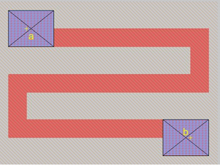
I did it finally and got the post-layout simulation results aligning to the pre-layout.
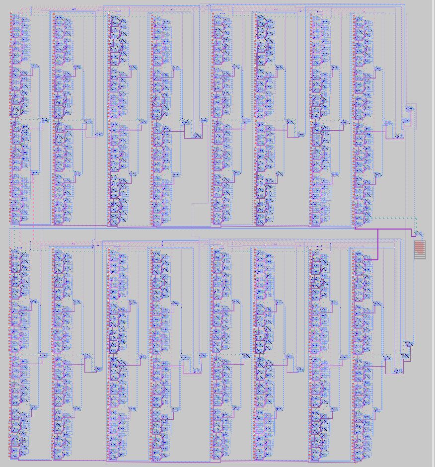
The next layout images shown are of 10-bit dac sub circuit using 2-bit DAC sub circuit logic.
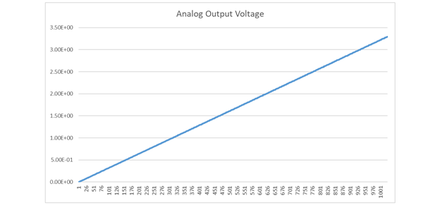
The next graph shown is the post-layout simulation graph of Vout v/s Digital Code for 10-Bit DAC.
The next graph shown is of the INL(LSB) v/s Digital Code Graph for 10-Bit DAC in post-layout.
The next graph shown is of DNL(LSB) v/s Digital Code Graph for 10-Bit DAC in postlayout.
 Due to this, I also got the opportunity to present this design at the VSD Open Conference, 2020. 2020 – VLSI System Design

Finally, I would like to say that, by following a top-to-bottom approach to do any project along with a mentor’s guidance, we can learn things quickly.
Thanks for reading!
Refer to GitHub Repo : https://github.com/xzlashutosh/avsddac_3v3
![]()
