This blog is regarding abstract submission for VSDOpen2018, which is the first online conference in VLSI, that covers all aspects of semiconductor technology with prime focus to build SoC using RISC-V CPU by illustrating exciting ways using (only) opensource EDA tools.
This conference has 6 symposium, out of which sixth symposium is to come up with innovative ways of laying out and characterizing complex cells for best performance. List of other symposium and session chair can be found in below link:
https://www.vlsisystemdesign.com/vsdopen2018-2/
This blog is about Symposium VI – Standard cell layout/characterization (abstract submission last date is 15th August, please see above link for details)
Let’s look int CCS/ECS timing model generation using GUNA characterization software:
Request for lab access by filling up form in below link:
https://www.paripath.com/cloud/guna-ide
Once you request gets approved, and you have lab access, below window is what you will see:
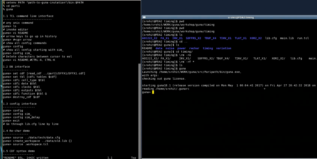
In above shell, you can type in commands like “vi README”, “ls”, and all unix commands. For more details about how to use the lab for experiments, you can refer to below course:
https://www.udemy.com/vsd-library-characterization-and-modelling-part-2/?couponCode=SYMPOSIUM_VI
Now, let’s see labs for creating CCS/ECS models. Open lib.cfg in your work area and modify the below variable to add models
config liberty_models {nldm ccs_timing ecsm_timing}
We will do all above together and run guna using below command
>guna run.tcl (Find more about run.tcl and the command guna in above course)
This will take some time and we are only running with default slope and load so that the simulation doesn’t take long. Hence, instead of table of 3×3 or 5×5, which you might have generally seen in timing libs, we will see one number and one waveform as shown below for a tri-state cell:
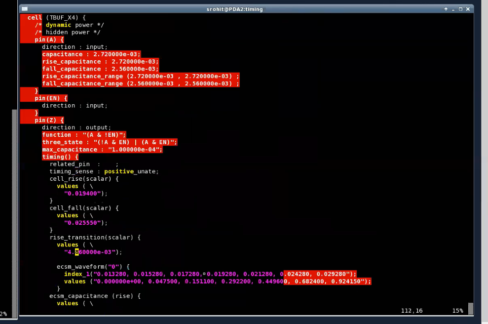
ECSM puts its number in the same arc as NLDM. The numbers you see in above image, below the cell_rise, cell_fall, rise_transition is all NLDM information. Under rise_transition, you will have ecsm_waveform and ecsm_capacitance. Now this is only one waveform, because we gave it only one load and one slope, just like we have one value under “rise_transition”. If we had 3×3 under rise_transition, then you would have had ecsm_waveform(“0”), ecsm_waveform(“1”), till ecsm_waveform(“8”), essentially 9 waveforms. And same thing with capacitance
Let’s look at CCS model:
Above is your ccs model. Receiver model is specified with receiver_capacitance1_rise (RC1R) and receiver_capacitance2_rise (RC2R). RC1R is the first part where it covers capacitance from 10% to 50% (or 20% to 50%) of the waveform and RC2R is the second portion which is 50% to 90% (or 50% to 80%). RC1R and RC2R combined, they make the entire rise_transition capacitance. Same with capacitance_fall.
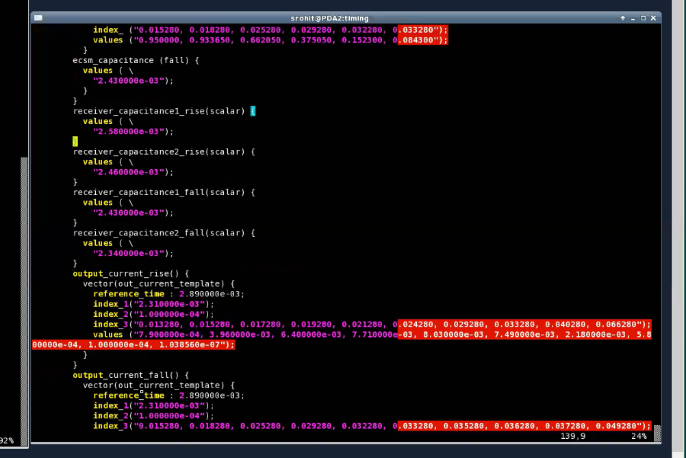
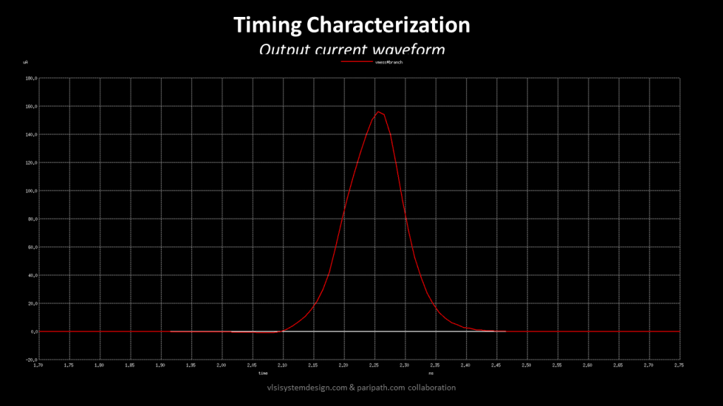
Just below receiver model, you will see driver model (output_current_rise and output_current_fall). Again, we will see only one waveform here. The vector which is you see under vector(out_current_template) is essentially your waveform. index_1 is your slope, index_2 is your load, index_3 is your time. And reference_time is where your sampling starts. The numbers in “values” section is your current waveform. Starts with e-04, from where it goes up, like a bell-shaped curve, till e-03, and goes all the way up till 2.2mA which is the peak and then it comes down to e-07 (like below image). For more details about this topic refer to my course on Library characterization Part 1 (concepts and SPICE only):
https://www.udemy.com/vlsi-academy-library-characterization-part-1/?couponCode=SYMPOSIUM_VI
Output current fall will be exactly the reverse of what is shown above. Hence, for output_current_fall, you will see the negative numbers. That’s your CCS driver model
Just in similar fashion, you can take up an idea of any complex cell, login to your Paripath account, access GUNA, produce results, optimize your cell for best PPA (may be modify the SPICE netlist for W and L) and share them in the online conference using below link:
https://www.vlsisystemdesign.com/vsdopen2018-2/
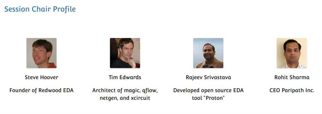
All your ideas will be reviewed by below panel of session chairs (who are all experts in their domains) and you might just get a chance to showcase your innovation to top crowd from VLSI industries:
The reason for this conference is to do out-of-the-box things in field of VLSI, to showcase your versatility and talent to a lot of TOP people, and get their attention, all online.
“This can be your new creative resume”
All the best for your submissions and happy learning
