Hello
Hope you had a great weekend! I didn’t had one, as was busy preparing high quality videos on Circuit design and SPICE simulations, which will be my 5th official VLSI course on Udemy. Yayyyyy !!
But why am I doing this….? I think, till now, after reading so many of my posts, you must have realized, its really the small transistors that’s driving semiconductor industry, and without knowing how they behave, its really no fun working in this industry. So, I had fun over the weekend preparing them. 🙂
Last post, I, indirectly introduced the concept of ‘drive strength’. Its basically, how resistive the PMOS or NMOS is?.
You can also find details about the ‘drive strength’ in my Signal Integrity Course on Udemy

In this one, I have represented resistance by a box. Wider the box, least is the resistance, more area available for current to flow from supply to output load, and hence faster it will charge the output load.
Did you notice one thing ? Due to wide box, these kind of transistors are larger in size, and hence occupy lot of area on chip.
Also the impact of having these kind of devices as the aggressor, makes ‘A’ so strong that it is able to charge the coupling cap very fast, thus producing the maximum glitch height.
So, one way to reduce glitch, is to …… (sentence continued after the below image)


(…… continued from above) reduce the drive strength of aggressor inverter. There are few more advantages of doing this. These transistors are smaller in size, so low overall chip area, thus packing more devices onto the same area.
What about victim? Its exactly reverse. The inverter needs to be strong to retain the logic level on victim net and reduce glitch.


So, looks like, we are back to square one. We save area in the aggressor side, while increase area on the victim side … Grrrhhhhh….. What to do? Let’s build a conclusion here in below image
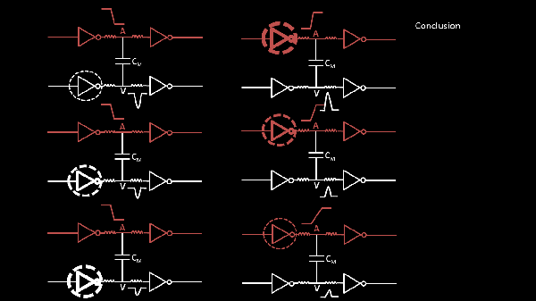
You need to optimize/adjust the inverter sizes in such a fashion, that the area will be optimum and affect of glitch in minimum. I gave a ready made image above, which can be directly used in your real designs to find the optimum size of inverter to reduce glitch, while maintaining optimum area.
We can’t eliminate glitch, but always can reduce it and avoid it by some smart techniques, like one shown above. There are great deal of techniques you can use to reduce glitch, and that makes the Signal Integrity and Crosstalk a really vast area of research.
Unfortunately, this topic can’t be completed in just 3 posts, but I think, I have done reasonably good job in introducing Signal Integrity, so that now, we start taking this seriuosly :), which, if ignored, will hit you hard, very hard. This message comes from experience and “Experience is what you get when you didn’t get what you wanted. And experience is often the most valuable thing you have to offer.”
Take it from me … I am giving it for FREE 🙂
Thanks
Kunal
