Hello
I feel lucky and blessed, after my last post on “Regular buffer v/s Clock buffer – Part 1“, as I received couple of emails, mentioning, this topic had been a problem in understanding, and the last post really helped them. I would like to Thank You all for appreciating it.
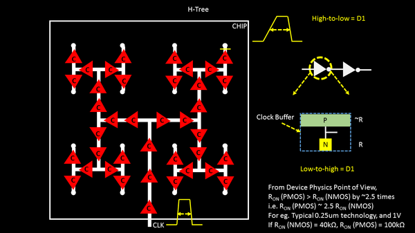
Coming back, whatever we mentioned about NMOS/PMOS resistances, lets use a few images to show the same.
We will replace resistance by a hollow box, bigger the box, more items can go through it (low resistance), and vise-versa (high resistance).
NMOS has a resistance ‘R’ and PMOS has higher resistance, ‘2.5R’

And this will be your buffer (regular) size

The size looks decent enough, and can be used on non-critical paths, like data-paths. But definitely cant be used for clock path, due the un-equal rise/fall times, which is due to the difference in resistances.
Hmmm…
Looks like, we need to fix this resistance to use this one in clock path. Lets use a bigger hollow box for PMOS

Hey, the resistance just reduced for PMOS, as we increased the width of hollow box. Technically, this ‘width’ is the channel width (W).
BUT, did you notice, we just increased the size of buffer. Bigger buffer, big chip area, $$$ reduced. Nobody wants to use a smart phone of a size of walkie/talkie.
You know what, its ok to increase the size a little bit, because performance, speed, accuracy are equally important. We will get back on how to smartly build the clock tree
Let’e increase the width even more, such that, the PMOS resistance matches NMOS resistance

Now, lets observe the high-to-low delay.….. (sentence continued after this image)

….. (continued from above) and low-to-high delay


The only price paid using these buffers are
1) bigger in size, so overall chip area increases
2) Very leaky, so should be carefully used, and not heavily
Warren Buffet had mentioned in one of his books “Price is what you pay. Value is what you get”
Performance is “Valuable” to customers. You don’t want a phone which takes hours to open an app, Do you ?
Thanks
Kunal
