Hi
I am happy to say, they really are connected….Let’s figure out how?
If you see a classic application of tri-state buffer, it’s the memory read-write operation, as shown below:
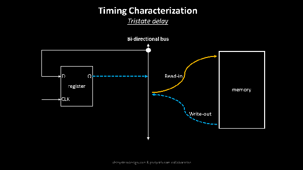
When we are trying to write into the memory from register, it’s a ‘read’ operation for memory (now all memory designers out there, this is the bare minimum explanation that I am providing, so bare me if I am excluding some details) In a memory-read operation, the register writes on the bi-directional bus, so register is on ‘out’ mode, whereas the memory reads in the data from bus, so its in ‘in’ mode.
Consider another scenario, where register is in ‘out’ mode, and memory is also writing data on to the bus, so it’s also in ‘out’ mode. This is a situation where bus receives data from 2 ends and that’s not tolerable which corrupts data. So what do we do? Add another tristate buffer between the register out and bus, like below:
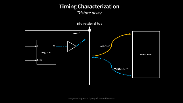
This simple arrangement solves problem of data corruption (at the cost of additional hardware). It looks simple in the above image, but it becomes a critical path, when you try to do an STA firm reg2mem path. Anyways, that can be handled.
Speaking of STA here, there is an additional requirement that comes along with tristate buffer..i.e. Library Characterization
So, additional cost involved in characterizing the buffer, but its also an interesting one. If you look into the interiors of tristate buffer, below is how it looks like:
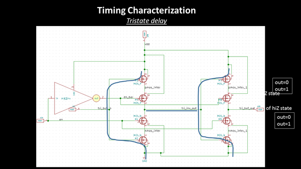
Woof…Looks like a complicated arrangement of transistors. It’s actually not complicated, but tricky. If you closely look above, we have back to back inverters connected, and in between top and bottom pmos/nmos transistors, we have another pmos/nmos transitors, whose inputs are connected to ‘en’ and ‘en_bar’. That’s the key. When ‘en’ is ‘0’, ‘en_bar’ is ‘1’, and the middle nmos and pmos are off. That makes complete buffer in open state. This state is called ‘high impedance state’, so the input data do not traverse to output. While when ‘en’ is ‘1’, ‘en_bar’ is ‘0’ your both nmos and pmos turns ‘on’, and the entire circuit behaves as if 2 back to back inverters are connected to form a buffer.
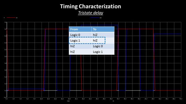
Characterizing a library for tristate buffer is not the usual way. Over here you find 4 different transitions. And below is the SPICE simulated waveform for tristate buffer along with 4 different transitions
Here on, the steps are simple.
Obtain or characterize the tristate buffer to measure slew or transitions for above 4 states, plug the tristate buffer and its library between your register and memory into your synthesized netlist and check for correct functionality
PNR tristate buffer and characterize it again for extracted tristate library, and use this new library for STA
You are done…Simple…
Looking at above approach of solving problems, reminds me of an interesting quote from Albert Einstein, “The formulation of a problem is often more essential that its solution, which may be merely a matter of mathematical or experimental skills”
I am proud to say, all my online courses focus on this skill of problem solving….Here’s the link:
So keep learning, keep formulating and I will see you in class…..Happy Learning!!
