Hey There,
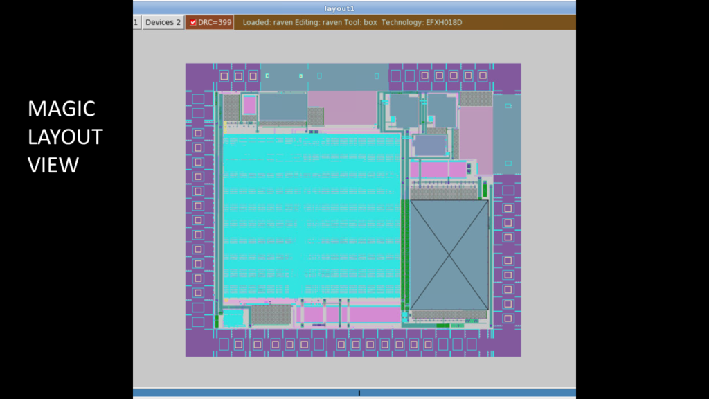
Now that it’s clear, that we can tapeout using open-source EDA tools (referring to recent RavenSoC tapeout by Efabless Corp. Pvt. Ltd. using XFAB 180nm technology node, see above pic), I think there will be more and more people using these tools, especially students, who can now learn entire VLSI backend using opensource EDA tools.
Now there will be lot of queries, so I thought of starting FAQ section for everyone who will be using MAGIC VLSI Layout tool. These are real-time LIVE conversations, which many people have emailed to me and Tim Edwards (SVP of Analog Platform, Efabless Corp. Pvt. Ltd.), and we have been consistently replying them. Hope you find them useful. Will be adding more FAQ’s in upcoming days
Question) Why doesn’t psubstratecontact and nsubstratecontact, which are defined in below ’tile’ section of tech file, appears in ‘contact’ section of tech file?
active psubstratepcontact,pohmiccontact,poc,pwcontact,pwc,psc
active nsubstratencontact,nohmiccontact,noc,nwcontact,nwc,nsc
Answer) Don’t they? The standard scmos.tech file has:
nsc nsd metal1
psc psd metal1
Sometimes it’s hard to see because magic uses all these aliases for names. If you have a techfile that’s missing something from the contact section, it’s possible to define a contact just with the
connectivity (i.e., in the “connect” section). The main difference is that the “contact” section handles all the varieties of the paint/erase tables. A contact defined without using “contact” will have all sorts of strange behavior when you select it and start moving or stretching it, or deleting it.
Question) I see in tech file, the tile type psd is “psubstratepdiff” and nsd is “nsubstratendiff”
active psubstratepdiff,pohmicdiff,pod,ppdiff,ppd,psd
active nsubstratendiff,nohmicdiff,nod,nndiff,nnd,nsd
Is it an overlap tile between “psubstrate and ndiff” and “nsubstrate and pdiff”?
Shouldn’t it be psd = psubstratendiff and nsd = nsubstratepdiff ?
Answer) No, psd is pdiff in psubstrate (i.e., P+) and nsd is ndiff in nwell (i.e., N+). These are the traditional names in scmos.tech. I also find them confusing and think that they should just be called “pplus” and “nplus”. I have not heard anyone use the term “ohmic diffusion” outside of Magic
techfiles and documentation, that I recall.
Question) Ok
So in a twin-tub CMOS process, ‘nsd’ and ‘psd’ are the ‘tubs’ or ‘wells’ inside which we build nmos/pmos, right?
Naming convention is confusing, as I haven’t heard of ‘ndiff’ in ‘nwell’ or ‘pdiff’ in psubstrate. Its the other way round in fabrication, right?
Answer) Part of the confusion is because most layout editors, because they have a very mask-centric representation, only show “active”, and then have other boxes representing “wells” and “implants”. Magic is different because it likes to show a more functional view, and sometimes you don’t
see the mask layers at all. Implant layers (P+ implant, N+ implant) are usually not shown. Instead, there are four kinds of diffusion shown:
“pdiff” is diffusion with P+ implant inside N-well
“ndiff” is diffusion with N+ implant in P-substrate (or P-well)
“psd” is diffusion with P+ implant in P-substrate (or P-well)
“nsd” is diffusion with N+ implant inside N-well.
So “psd” is the P-substrate (or P-well) tap, usually tied to ground, and “nsd” is the N-well tap, usually tied to VDD.
A twin-tub process may or may not show “pwell” explicitly, as the mask may be defined as (NOT nwell). By having different types for “ndiff” and “pdiff”, magic allows a layout to be drawn with no wells at all—it will figure out where the wells are from where the ndiff and pdiff are, and automatically generate them (I might also add that this is dangerously prone to error, and nobody does it that way).
All above conversation and many more has been captured in a more structured form, in my below online course:
https://www.udemy.com/vlsi-academy-custom-layout/?couponCode=FAQ_MAGIC
Look for more FAQ’s coming up…All the best and happy learning….


