Talking about leakage power or static power, one classic definition that comes into our minds is that of sub-threshold leakage current, which can be replicated or explained through below image
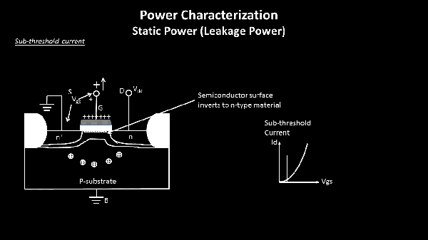
It basically says, that your transistor cannot be turned off so easily, just by bringing down your gate-to-source voltage Vgs below threshold voltage Vt. Converting a small area beneath gate region into a n-type channel is easy. But to convert that small area back to p-type is difficult, and you will still see some electrons in the channel area even when your Vgs < Vt i.e. in sub-threshold region, hence you see a small amount of current flowing even when transistor is completely OFF. That’s sub-threshold current
That was easy and might be a known fact to most of you. Let’s unearth what might seem something new, but has been there around for long time – Junction leakage current and Tunneling current. These additional currents are also a source of leakage power, so let me try to explain them through below images:
Junction leakage current:
If you see the below image, the n+ source and drain area forms a PN junction diode with P-substrate, and due to difference in doping concentration levels of n+ and P-substrate, there is a concentration gradient due to which we see an additional current from n+ diffusion to the substrate, which is called the junction leakage current. Since your transistor is OFF, the diode is reverse biased, and the current that you see is the reverse saturation current of diode
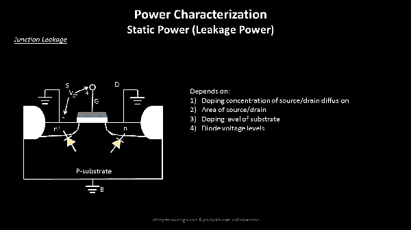
Again, the junction leakage current depends on several factors like doping concentration of source/drain and substrate, diode voltage levels and area of source and drain. And additional current is additional power which needs to be accounted for
Tunneling current:
The explanation of tunneling current needs a knowledge on energy band diagrams of a MOS capacitor system as shown below:
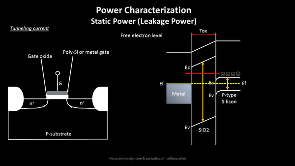
So, in a MOS system, the metal gate and P-type silicon has fermi energy level, which are at different energy values. Now when 2 different systems with 2 different fermi levels are connected across SiO2, at thermal equilibrium when there are no currents flowing, the fermi-level of all the components attached are expected to be at same level, and while that process, the energy band of P-type silicon at the Oxide-semiconductor interface tends to bend. This band bending actually, from abstract level, is the small region under the gate region which converts to n-type. Now depending on the oxide thickness Tox, there is a higher possibility of electrons in p-type substrate near the interface, to just tunnel through the oxide and enter into gate regions, resulting in gate leakage current.
Again, where there is current, there is an additional power. Surprisingly, if you have been analyzing power in your work place, these numbers are already quoted in your libraries (I will show in my next blog), and you have been taking into account of the leakage power. Now with this blog, things might have just become more transparent to you. More transparent the system is, more interesting it becomes to solve a problem
Have you ever heard of “Good design is obvious, Great design is transparent”.
Now the question is, do you want to be a good designer or great designer?
Happy Learning !!
