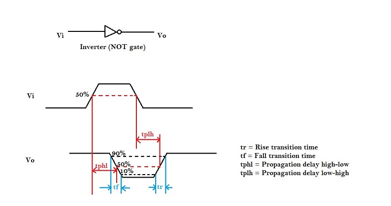
The propagation delay of a logic gate e.g. inverter is the difference in time (calculated at 50% of input-output transition), when output switches, after application of input.
In the above figure, there are 4 timing parameters. Rise time (tr) is the time, during transition, when output switches from 10% to 90% of the maximum value. Fall time (tf) is the time, during transition, when output switches from 90% to 10% of the maximum value. Many designs could also prefer 30% to 70% for rise time and 70% to 30% for fall time. It could vary upto different designs.
The propagation delay high to low (tpHL) is the delay when output switches from high-to-low, after input switches from low-to-high. The delay is usually calculated at 50% point of input-output switching, as shown in above figure.
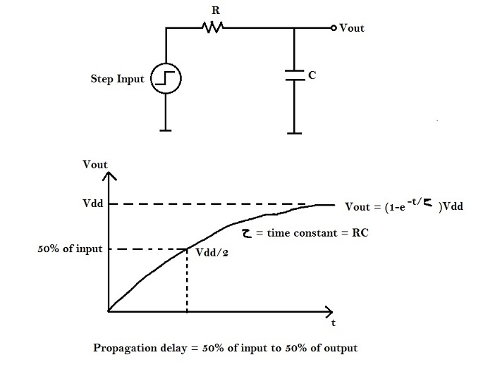
Now, in order to find the propagation delay, we need a model that matches the delay of inverter. As we have seen above, the switching behavior of CMOS inverter could be modeled as a resistance Ron with a capacitor CL, a simple first order analysis of RC network will help us to model the propagation delay.
Consider the following RC network to which we apply a step input.
Our aim is to find ‘t’ at Vdd / 2. Vout = (1-e-t/τ) Vdd, where τ = RC = time constant. Substituting ‘Vout’ equal to Vdd/2, and ‘t’ equal to ‘tp’ in above equation, we get the following : Vdd/2 = (1-e-tp/τ) Vdd Therefore, tp = ln(2) τ = 0.69τ Hence, tp = 0.69RC Hence, a CMOS inverter can be modeled as an RC network, where R = Average ‘ON’ resistance of transistor C = Output Capacitance
Engineering Change Order (ECO) is the process of modifying the PNR netlist in order to meet timing (i.e. setup, hold, transition and max_capacitance) requirements. For eg. if there’s a setup violation in the design, it implies that a combinational path has large delay than required. In this case, you need to reduce the delay by up sizing cell, which reduces resistance, in turn, reduces RC delay of the path.
Following sections explains the concepts needed to modify delay of a particular logic cell. Inverter has been considered as an example.
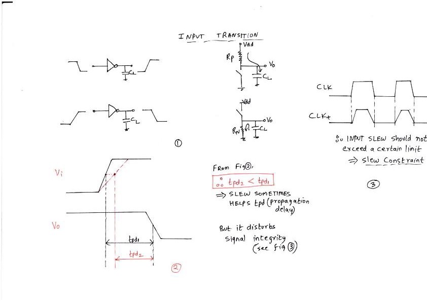
Below figure shows that the output capacitance (CL) of an inverter is constant, and the input slew is varying.
From the above figure, if input transition is high, it helps or reduces the propagation delay. But, on the other hand, it disturbs signal integrity. This implies, the circuit should not be over-designed i.e. if a circuit could run at an input transition of 50 ps, it should not be designed to run at 20 ps.
“Delay reduces with increase in input transition and constant load capacitance”
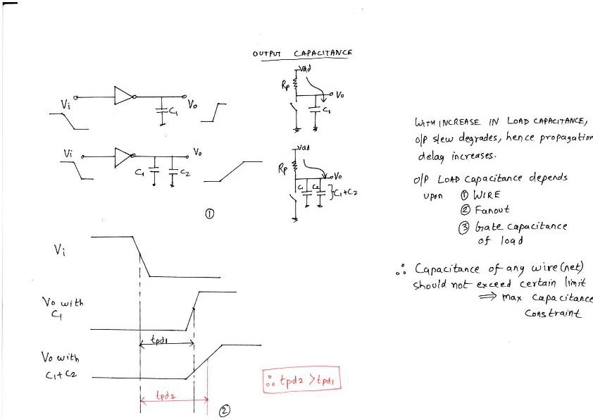
Consider, another scenario, where input transition is constant, whereas, output capacitance is varying. This is captured in the following diagram
As shown in the above figure, as output capacitance increases, the total time required to charge this capacitance increases, hence RC delay increases. This could be helpful in fixing hold violations where delay needs to be increased to meet hold margin.
“Delay increases with increase in output capacitance and constant input transition”
The above two examples shows that the delay of cell directly depends on input transition and output capacitance.
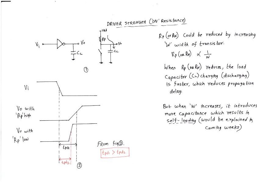
Another technique to modify the delay of cell is to ‘upsize’ or ‘downsize’ a cell i.e. varying the drive strength (‘ON’ resistance) of the cell. This is captured in the figure below
High drive strength cell indicates a cell having low ‘ON’ resistance. Due to low resistance, the time required to charge the output capacitance will be low, i.e. RC delay reduces. This technique is useful to fix setup violation where the delay needs to reduced. The inverse (i.e. high ‘ON’ resistance) is useful for fixing hold violation, where the delay needs to increased.
“Delay varies by varying drive-strength (ON resistance) of the logic cell”
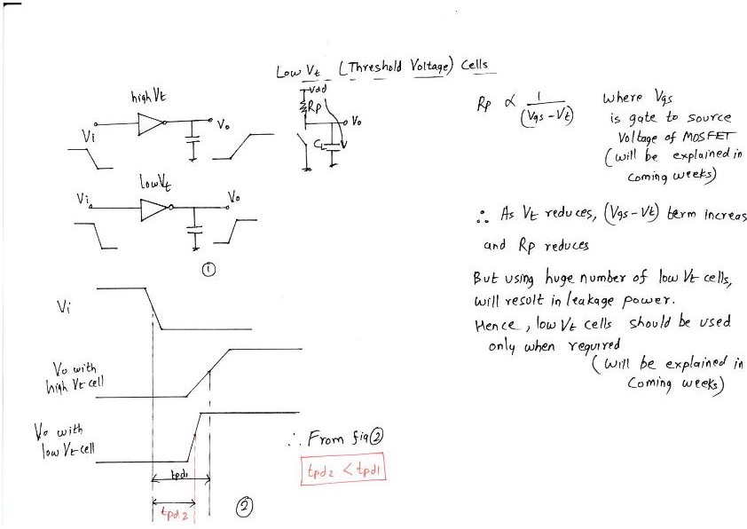
Another intelligent method, but a leaky one, to reduce the delay of cell is to swap high threshold voltage (Vt) cell with low Vt cell. Refer to the below diagram
The characteristics of NMOS (or PMOS) device is such that, the ‘ON’ resistance is inversely proportional to (Vgs – Vt). But, the direct effect is that low Vt cells are often more leaky i.e. leakage power increases.
“Delay can be reduced by using low Vt cells, but the cost paid is high leakage power”
VSDSquadron, a cutting-edge development board based on the RISC-V architecture that is fully open-source. This board presents an exceptional opportunity for individuals to learn about RISC-V and VLSI chip design utilizing only open-source tools, starting from the RTL and extending all the way to the GDSII. The possibilities for learning and advancement with this technology are limitless.
Furthermore, the RISC-V chips on these boards should be open for VLSI chip design learning, allowing you to explore PNR, standard cells, and layout design. And guess what? vsdsquadron is the perfect solution for all your needs! With its comprehensive documentation and scalable labs, thousands of students can learn and grow together.
With VSD Hardware Design Program (VSD-HDP), you have the opportunity to push the boundaries of what exist in open source and establish the new benchmark for tomorrow.
It will leverage your degree in Electrical or Computer Engineering to work with
Programmable logic
Analog/ digital IP
RISC-V
Architecture & microprocessors
ASICs and SoCs on high-density digital or RF circuit cards
Gain hands-on knowledge during design validation and system integration.
Sounds exciting to just get started with expert mentors, doesn’t it? But we are looking for the next generation of learners, inventors, rebels, risk takers, and pioneers.
“Spend your summer working in the future !!”
Outcomes of VSD Online Research IP Design Internship Program
Job opportunities in Semiconductor Industry
Research work can be submitted to VLSI International journals
Participate in Semiconductor International Conference with Internship Research Work
Paper Publications in IEEE Conference and SIG groups
Tape out opportunity and IP Royalty
Interact with world class Semiconductor designer and researchers
Academic professions where more research projects are encouraged.
All the above research and publication work will help colleges and institutes to improve accreditation levels.
VSD – Intelligent Assessment Technology (VSD-IAT) is expertly built training platform and is suited for designer requirements. Semiconductor companies understand the value of training automation and Engineer performance enhancement, and do not need to be convinced of the impact of a virtual platform for learning. VSD trainings are quick, relevant, and easy to access from any device at any time zone.
VSD Intern Webinars
VSD Interns made it happen !!
VSD is working towards creating innovative talent pool who are ready to develop design and products for the new tech world. VSD believes in “Learning by doing principle” , and always prepare the student to apply the knowledge learned in the workshops, webinars and courses. We always push our students to work on new designs, test it and work continuously till it becomes the best performing design. Any student who enrolls to VSD community starts working with small design and grows with us and develops a tapeout level design with complete honesty and dedication towards the Work !!
Welcome to the World’s only online conference in Semiconductor Industry VSDOpen Conference. With enormous support and global presence of audience from different segments of industrial lobby and academia made a highly successful event. Evolution is change in the genetic makeup of a population over time, online conference is one kind evaluation everyone adapt soon.
VSDOpen 2022 is an online conference to share open-source research with the community and promote hardware design mostly done by the student community.
VSDOpen 2022 is based on the theme “How to lower the cost to learn, build, and tapeout chips ?” , which will provide a platform to community to build stronger designs and strengthen the future of Chip design.
VSDOpen is envisioned to create a community based revolution in semiconductor hardware technology.
The open source attitude is required to bring out the talent and innovation from the community who are in remote part of world and have least access to the technologies. And now Google support will help to bring the vision to execution by VSD team.
VSD Online Course by Kunal Ghosh
VSD offers online course in complete spectrum of vlsi backend flow from RTL design, synthesis and Verification, SoC planning and design, Sign-off analysis, IP Design, CAD/EDA automation and basic UNIX/IT, Introduction to latest technology – RISC-V, Machine intelligence in EDA/CAD, VLSI Interview FAQ’s.
Current Reach – As of 2021, VSD and its partners have released 41 online VLSI courses and was successfully able to teach ~35900 Unique students around 151 countries in 47 different languages, through its unique info-graphical and technology mediated learning methods.