I am hidden, but I exist-Dynamic power dissipation in CMOS

Meet me, I am “hidden power”

Dynamic power dissipation in CMOS

When we are asked about dynamic power dissipation, below 2 things just appear at the top of our mind:

Switching power dissipation

The word ‘switching’ over here means a lot. It’s not just that inputs are switching, it’s the outputs also. Now why do I stress on the word outputs also’? That’s because, there’s also power dissipation that happens while inputs switch and outputs do not switch. Stay with me, I will introduce it just after this section.Coming back to switching power dissipation, take the below example:

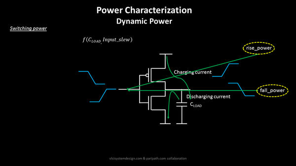
So here, whenever your input switches from logic 1 to logic 0, the output switches from logic 0 to logic 1 and you see charging current flowing from Vdd to CLOAD which results to rise_power (this is a liberty attribute used to denote rise_power). And vice-versa holds true when input switches from logic 1 to logic 0
This was easy…Next, there is another kind of power that dissipates when your inputs and outputs are switching, that’s short-circuit power

Short circuit power dissipation in CMOS inverter
This power dissipation is another beast. Look at below image:
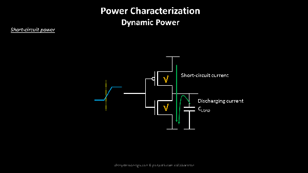
When your input is at logic ‘0’ and assuming your VDD is at 1.8V (considering it’s a 180nm technology node), why do you think, from physics point of view, does your PMOS turns ON? The reason is, logic ‘0’ at gate means its at 0V, Vdd is at 1.8V, the PMOS Vgs = 0 – 1.8 = -1.8v which is far above the threshold voltage of PMOS transistor, which makes the PMOS to turn ON
Similarly, Vgs of NMOS is 0V – 0V = 0V, which is below the threshold voltage of NMOS transistor and hence NMOS is OFF. Now look at the highlighted area in the input transitioning waveform. In that area, if gate input rises from 0v to (say) 0.5v, the Vgs of NMOS is 0.5v, which is just above the threshold voltage of NMOS (assuming NMOS Vt is 0.2V for 180nm technology node), so it just turns ON
Now the Vgs of PMOS is roughly, say 0.5v – 1.8v = -1.3V which is again, far above threshold voltage of PMOS transistor, so your PMOS transistor is still ON. You see, at this point, both PMOS and NMOS transistor are ON. Looking Vdd at higher potential, and GND at lower potential, there is now a direct path from Vdd to Gnd.

That’s short circuit current, and hence the name short-circuits power dissipation

So now the big question? What if the outputs do not switch, while only the inputs switch, like the below case of AND gate
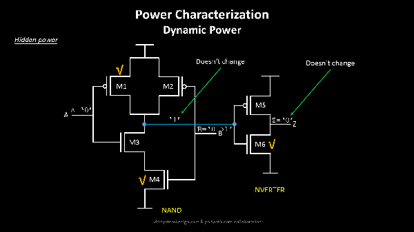
Here, if you see, even though your input ‘B’ switches from logic ‘0’ to logic ‘1’, your NAND output and hence, the AND output doesn’t switch. So do we still see power dissipation in these kind of scenarios?

Hidden power

That’s me…”hidden power”. That’s how I introduced myself in the beginning of the post. Now even though, in the above image, the outputs do not switch, the switching of input ‘B’ creates a unique path for current flow from Vdd to Gnd. Look at below image:
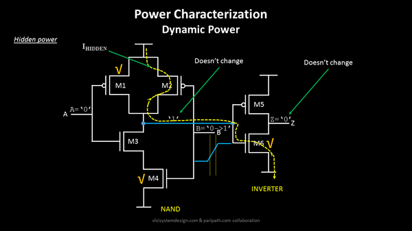
During the transitioning of ‘B’, due to similar reasons of Vgs being greater than threshold voltage of PMOS and NMOS transistors, M2 is ON momentarily, and I flow from Vdd – M2 – M6 – GND. Since I am hidden inside the boundary of the cell, the name hidden power
This brings me to very important point about myself, that if I am hidden, doesn’t mean I do not exist…

Language exerts hidden power, like the moon on the tides” – Rita Mae Brown

Happy Learning !!

Registration for Ethical RISC-V IoT Workshop

Welcome to Ethical RISC-V IoT Workshop

The “Ethical RISC-V IoT Workshop” at IIIT Bangalore, organized in collaboration with VSD, is a structured, educational competition aimed at exploring real-world challenges in IoT and embedded systems. Participants progress through three stages: building an application, injecting and managing faults, and enhancing application security. The event spans from May 9 to June 15, 2024, culminating in a showcase of top innovations and an award ceremony. This hands-on hackathon emphasizes learning, testing, and securing applications in a collaborative and competitive environment.

Rules :
  1. Only for Indian Student whose college is registered under VTU
  2. Only team of 2 members can Register
  3. Use only VSDSquadron Mini resources for product development
Awards :
  1. Prize money for final 10 Team
  2. 3 Winner team’s Product will be evaluated for Incubation
  3. 7 consolation prizes
  4. Completion Certificate to final round qualifier
  5. Chance to build a Proud Secured RISC-V Platform for India

Date for Registration : 9th May - 22nd May, 2024
Hackathon Inauguration : 23rd May 2024

VSDSquadron (Educational Board)

VSDSquadron, a cutting-edge development board based on the RISC-V architecture that is fully open-source. This board presents an exceptional opportunity for individuals to learn about RISC-V and VLSI chip design utilizing only open-source tools, starting from the RTL and extending all the way to the GDSII. The possibilities for learning and advancement with this technology are limitless.

Furthermore, the RISC-V chips on these boards should be open for VLSI chip design learning, allowing you to explore PNR, standard cells, and layout design. And guess what? vsdsquadron is the perfect solution for all your needs! With its comprehensive documentation and scalable labs, thousands of students can learn and grow together.

VSD HDP (Hardware Design Program) Duration-10 Week

With VSD Hardware Design Program (VSD-HDP),  you have the opportunity to push the boundaries of what exist in open source and establish the new benchmark for tomorrow.

It will leverage your degree in Electrical or Computer Engineering to work with

  • Programmable logic
  • Analog/ digital IP
  • RISC-V
  • Architecture & microprocessors
  • ASICs and SoCs on high-density digital or RF circuit cards
  • Gain hands-on knowledge during design validation and system integration.

Sounds exciting to just get started with expert mentors, doesn’t it? But we are looking for the next generation of learners, inventors, rebels, risk takers, and pioneers.

“Spend your summer working in the future !!”

Outcomes of VSD Online Research IP Design Internship Program

  1. Job opportunities in Semiconductor Industry
  2. Research work can be submitted to VLSI International journals
  3. Participate in Semiconductor International Conference with Internship Research Work
  4. Paper Publications in IEEE Conference and SIG groups
  5. Tape out opportunity and IP Royalty
  6. Interact with world class Semiconductor designer and researchers
  7. Academic professions where more research projects are encouraged.
  8. All the above research and publication work will help colleges and institutes to improve accreditation levels.

Know More Information

VSD – Intelligent Assessment Technology (VSD-IAT)

VSD – Intelligent Assessment Technology (VSD-IAT) is expertly built training platform and is suited for designer requirements. Semiconductor companies understand the value of training automation and Engineer performance enhancement, and do not need to be convinced of the impact of a virtual platform for learning. VSD trainings are quick, relevant, and easy to access from any device at any time zone.

VSD Intern Webinars

VSD Interns made it happen !!

VSD is working towards creating innovative talent pool who are ready to develop design and products for the new tech world. VSD believes in “Learning by doing principle” , and always prepare the student to apply the knowledge learned in the workshops, webinars and courses. We always push our students to work on new designs, test it and work continuously till it becomes the best performing design. Any student who enrolls to VSD community starts working with small design and grows with us and develops a tapeout level design with complete honesty and dedication towards the Work !!

Check out VSD Interns Achievement!

VSDOpen Online Conference

Welcome to the World’s only online conference in Semiconductor Industry VSDOpen Conference. With enormous support and global presence of audience from different segments of industrial lobby and academia made a highly successful event. Evolution is change in the genetic makeup of a population over time, online conference is one kind evaluation everyone adapt soon. 

  • VSDOpen 2022 is an online conference to share open-source research with the community and promote  hardware design mostly done by the student community.
  • VSDOpen 2022 is based on the theme “How to lower the cost to learn, build, and tapeout chips ?”  , which will provide a platform to community to build stronger designs and strengthen the future of Chip design.
  • VSDOpen is envisioned to create a community based revolution in semiconductor hardware technology.
  • The open source attitude is required to bring out the talent and innovation from the community who are in remote part of world and have least access to the technologies.  And now Google support will help to bring the vision to execution by VSD team

VSD Online Course by Kunal Ghosh

VSD offers online course in complete spectrum of vlsi backend flow from RTL design, synthesis and Verification, SoC planning and design, Sign-off analysis, IP Design, CAD/EDA automation and basic UNIX/IT, Introduction to latest technology – RISC-V, Machine intelligence in EDA/CAD, VLSI Interview FAQ’s.

Current Reach – As of 2021, VSD and its partners have released 41 online VLSI courses and was successfully able to teach  ~35900 Unique students around 151 countries in 47 different languages, through its unique info-graphical and technology mediated learning methods.

Enquiry Form