Switching Activity of CMOS
A CMOS, is basically an inverter logic (NOT gate), that consists of a PMOS at the top, and NMOS at the bottom (as shown in figure below), whose ‘gate’ and ‘drain’ terminal are tied together. The ‘gate’ terminals of both the MOS transistors is the input side of an inverter, whereas, the ‘drain’ terminals form the output side. The ‘source’ terminal of PMOS is connected to ‘Vdd’, whereas source of NMOS is connected to ‘Vss’, as shown below.
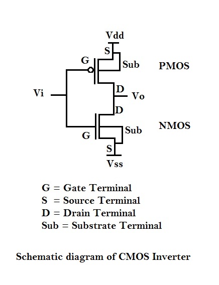
There’s a fourth terminal for a MOS transistor commonly referred to as ‘Substrate’ terminal. It is connected to ‘Vdd’ for PMOS and to ‘Vss’ for NMOS. This is one of the terminals of MOS transistor, which could to be used to vary the threshold voltage of transistor by applying certain voltage to it.
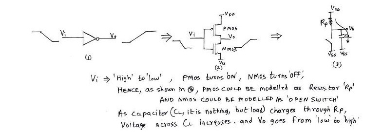
Now, let us look at the transient response of an inverter. Consider the following figure. When ‘Vi’ switches from high to low, PMOS turns ‘ON’ whereas NMOS turns ‘OFF’. During this operation of CMOS inverter, NMOS is modeled as an ‘open switch’, whereas PMOS is modeled as a resistance ‘Rp’ followed by a capacitor CL. In a large circuit, every CMOS is superseded and/or preceded by logic gates, which is again, nothing but a bunch of NMOS and PMOS transistors. These transistors contribute to lot of capacitance, which contribute to CL, load capacitance. Also, the wires connected to Vi and Vo of the inverter contribute to the load capacitance CL. Hence, during the above mode of operation, CL charges to Vdd, through Rp, and ‘Vo’ switches from logic ‘0’ to logic ‘1’.
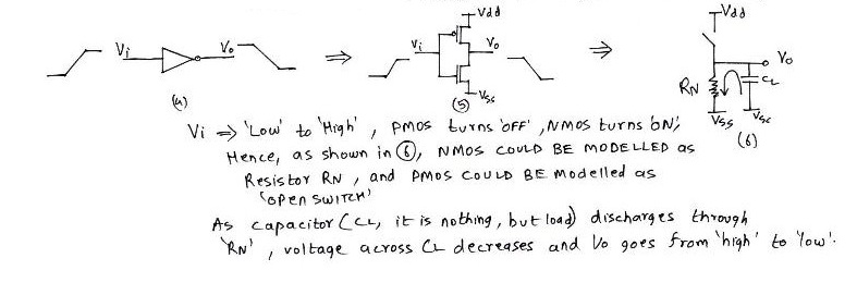
Now, when ‘Vi’ switches from low to high, PMOS turns ‘OFF’, whereas NMOS turns ‘ON’. This behavior could be modeled as an ‘open switch’ for PMOS and resistance ‘Rn’ for NMOS followed by a capacitor CL. Hence, during this mode of operation, CL discharges to Vss, through Rn, and ‘Vo’ switches from logic ‘1’ to logic ‘0’, as shown in figure below.
We understand that when ‘Vi’ switches from low to high (or high to low), ‘Vo’ switches from high to low (or low to high). But, ‘Vo’ doesn’t changes instantaneously, but after a finite amount of delay after application of ‘Vi’. The time required for change in ‘Vo’ after application of ‘Vi’, is called as propagation delay of the inverter. This would be more clear in the next section.
Propagation Delay of CMOS inverter
The propagation delay of a logic gate e.g. inverter is the difference in time (calculated at 50% of input-output transition), when output switches, after application of input.
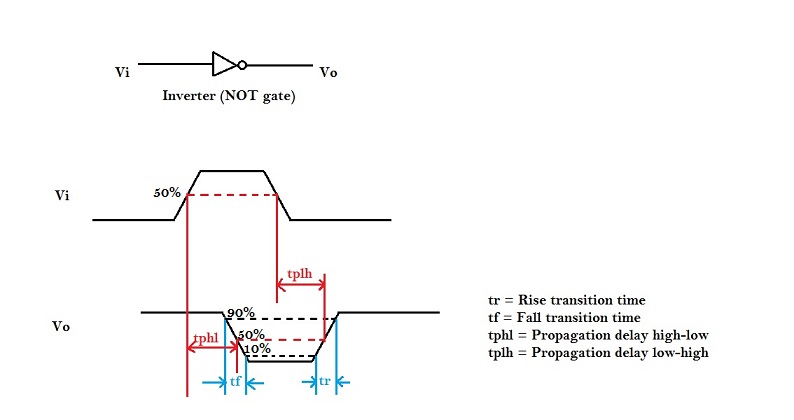
In the above figure, there are 4 timing parameters. Rise time (tr) is the time, during transition, when output switches from 10% to 90% of the maximum value. Fall time (tf) is the time, during transition, when output switches from 90% to 10% of the maximum value. Many designs could also prefer 30% to 70% for rise time and 70% to 30% for fall time. It could vary up to different designs.
The propagation delay high to low (tpHL) is the delay when output switches from high-to-low, after input switches from low-to-high. The delay is usually calculated at 50% point of input-output switching, as shown in above figure.
Now, in order to find the propagation delay, we need a model that matches the delay of inverter. As we have seen above, the switching behavior of CMOS inverter could be modeled as a resistance Ron with a capacitor CL, a simple first order analysis of RC network will help us to model the propagation delay.
First order RC network
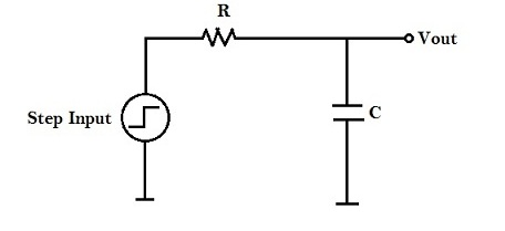
Consider the following RC network to which we apply a step input.
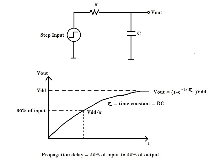
Our aim is to find ‘t’ at Vdd / 2.
Vout = (1-e-t/τ) Vdd, where τ = RC = time constant.
Substituting ‘Vout’ equal to Vdd/2, and ‘t’ equal to ‘tp’ in above equation, we get the following :
Vdd/2 = (1-e-tp/τ) Vdd
Therefore, tp = ln(2) τ = 0.69τ
Hence, tp = 0.69RC
Hence, a CMOS inverter can be modeled as an RC network, where
R = Average ‘ON’ resistance of transistor
C = Output Capacitance
Power Consumption
Consider the following scenario where output capacitor CL charge from 0 to ‘Vdd’ as input switches from ‘Vdd’ to ‘0’:
The charging and discharging current and voltage waveforms could be shown as below :
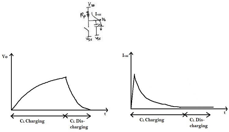
Hence, whenever output load CL gets charged from ‘0’ to ‘Vdd’, a finite amount of energy is drawn from the power supply. part of which is dissipated in Rp, whereas the remaining is stored in CL. The reverse happens whenever CL gets discharged from ‘Vdd’ to ‘0’i.e. the energy is dissipated in Rn.
The power consumed at any instance by a CMOS circuit is given by :
p(t) = v(t) * i(t) = Vsupply * i(t)
Now, in order to calculate the amount of energy during a single switching,refer to the following RC equivalent network for CMOS switching from ‘low’ to ‘high’
Energy = Power * Delay
Let E0->1 denote energy consumed whenever output switches from ‘0’ to ‘Vdd’.
Therefore,
E0->1 = ∫ p(t) . dt = Vdd ∫ idd (t) . dt = Vdd ∫ CL * Vdd . dVout = CL * Vdd2
(use the current-voltage relationship to understand the above integration i.e. C = Q / V = I*t / V )
Hence, every time a circuit switches, it consumes CL * Vdd2 amount of energy. Thus, amount of energy consumed, if a circuit (e.g. clock) switches ‘n’ times, will be n * CL * Vdd2 , which can gain attention.
