The release of the fully open-source Skywater 130nm PDK was a welcoming change, coupling it with open-source design tools it enabled just about anyone to work on real manufacturable designs at 130nm node. In this 8-week internship I spent the first week on researching existing work and making design decisions for the PLL components namely – Phase Frequency Detector, Charge Pump, Voltage Controlled Oscillator and Frequency Divider. I also looked into linking of the Sky130nm PDK with SPICE for the circuit implementation. Proceeding forward the the standard open-source tools ngspice & Magic was chosen for the spice circuit simulations and layout design respectively.

The regular design flow was followed. The circuit implementation to start off with, followed by the corresponding ngspice simulations and corrections to circuits. It was a tough challenge to implement a PLL circuit but at the same time an effective learning process. Then comes the backend – layout design followed by parasitic extraction (also available in Magic). Through this flow the regular loop back for corrections was required. Infact, going into post-layout simulations it was almost immediately clear that quite a bit of corrections in circuit and layout was needed and had to regress back and repeat the process until the result could meet the specifications. Initial specification was to achieve expected functionality (proper locking, good lock-time and low jitter) for a range of temperature for different corners. Taking up the whole design process it was seen more feasible in the available time to focus on just the ‘tt’ corner at room temperature.

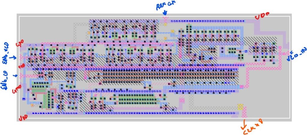
The finished PLL layout
It so happened that the Google-Skywater-Efabless MPW shuttle came at the right time, towards the end of the 8-week internship programme. It was unclear if a student like me would be able to meet the demands of something like a tapeout but still chose to give it the best try. Efabless oversaw the MPW shuttle and really made everything a lot easier for the community by providing the ‘Caravel’ template. What this meant is, all the testing, I/O and such infrastructure were already available on ‘Caravel’ and all that was required for the designer was to focus on properly integrating their design into the project area on the ‘Caravel’ chip. Not just that they provided the whole automated method to integrate the design layout onto the ‘Caravel’. This really shortened what would otherwise have been very tedious and complicated. Of course, it had its challenges at an individual level, community level and for Efabless to make the whole thing happen but timely efforts from them and the community made it a great experience. To attempt something like a tapeout would not have been possible if it weren’t for the efforts of Efabless, Skywater and Google. Also, I thank Kunal, VSD and the open-source VLSI community for facilitating this learning experience for me.

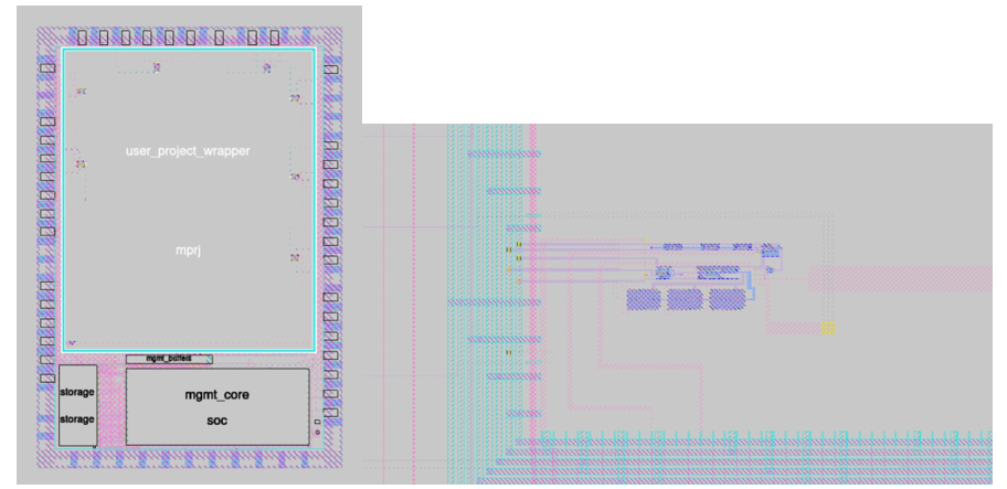
On the left: The Caravel chip, the large blank-looking space is the project area, the specs are the PLL (left bottom corner) and Opamps (Opamps from another designer).
On the right: Zoomed in on the PLL inside the Caravel, the thick horizontal and vertical rails are the power lines. There are also input and output pins along this periphery and the PLL inputs and outputs are connected to the appropriate ones from it.
GitHub Links:
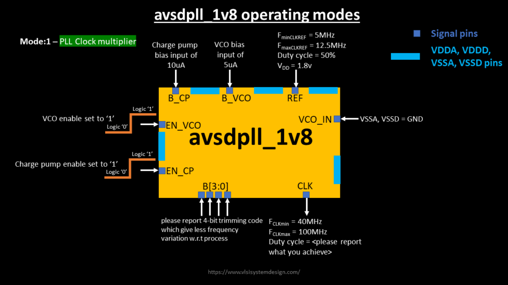
8x PLL Clock Multiplier IP with an input frequency range of 5Mhz to 12.5Mhz and output frequency range of 40Mhz to 100Mhz, giving a 8x multiplied clock at ~50% duty cycle on tt corner at room temperature.
https://github.com/lakshmi-sathi/avsdpll_1v8
41 forks.
121 stars.
1 open issues.
Recent commits:
- adding sim files from PDK, lakshmi-sathi
- edits for workshop, lakshmi-sathi
- schematic diagrams and latest tech file, lakshmi-sathi
- Update README.md, GitHub
- Update README.md, GitHub
Caravel is a standard SoC template with on chip resources to control and read/write operations from a user-dedicated space.
https://github.com/efabless/caravel
105 forks.
390 stars.
100 open issues.
Recent commits:
- Merge pull request #557 from efabless/add_mag_to_caravel_liteUpdate auto-update-caravel-lite.yml, GitHub
- Update auto-update-caravel-lite.yml, GitHub
- tag = 2024.09.12-1, GitHub
- Merge pull request #553 from efabless/reduced_poly_fillModifications to reduce poly fill and re-enable LVS., GitHub
- Added PDK path to first standard cell use statement, David Lindley
Related Posts:
- Accelerating the Future of Semiconductor Talent with…
- Secure Saiyan
- The Future of Chip Design: The Next Generation is…
- Real Time Implementation of BitNetMCU
- RISC-V Mini Game Console
- Shape Tomorrow’s Technology Today: ELCIA Hackathon…
- 40 Basic Questions to Prepare in Combinational Circuits
- LiFi Lock - An authentication system using LiFi…
- Smart Plant Care using the VSD_Squadron-MINI-BOARD
- COLORIMETER


