My biggest challenge – Do I have money to build better chips?

Hello

Of course …. The biggest cost that I am mentioning about is the fab cost and that’s my biggest challenge to build better chips. We all know that. But let’s talk about of some real numbers and facts here

When mentioned about fab cost, lithography accounts for a major portion of it (almost 32%) as shown in below image[1]. Though it’s really important to know what is ‘photo lithography’, I will briefly explain this, while focus mainly on the history of rise in fabrication cost

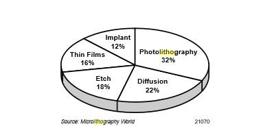
Photo lithography is a process to transfer geometric pattern from mask to wafer surface through a light sensitive chemical called as photo resist. There could be about 30-50 mask layers and each mask goes through a photo lithography process to fabricate a complex chip onto a silicon wafer i.e. a wafer goes through ~30 to 50 cycles of photo lithography [2]

Above image represents the split of fabrication cost per wafer. But, while building a semiconductor fabrication facility, apart the photo lithography equipment taking major plunge in cost, wafer size also dominates the increasing cost of fabrication.

How’s that so? Let me briefly explain this

A round wafer can hold more than 1000 die’s where a ‘die’ represents a fully functional chip. Below image shows a wafer map where each blue square represents a ‘die’

Bigger the wafer, more the number of die’s that can be accommodated and higher the throughput. When we move from 4inch to 6inch, that’s an 2.25times increase in the wafer area. Now that’s an ‘equivalent’ increase in cost per wafer and hence cost per mask. Carefully look into the below equations [4]:

So in order to keep a fab profitable, it should constantly operate at high volumes. TSMC’s initiative to build ‘gigafab’ will process around 100K ‘300mm’ wafers per month [5]. High volumes definitely reduce unit costs but fixed costs of building fabs has hit sky high over the period of last 20 years

Overall, to build a fab in 1966, it costs around $14M, which had increased to $1.5B by 1995, and today the cost of building a leading edge fab will be around $6B [6]

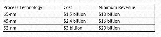
That’s not all. To add to the overall cost, there is an additional cost involved to develop basic process flow at each node. Over the years, industry has moved on from 0.5um technology to 0.065um and even lesser (0.016um). There is a cost involved in developing a process for each node that adds up the total cost of building a fab. Below table carefully sums up the cost involved in developing a process technology and minimum revenue needed to achieve an ROI at each node [7]. It means that to achieve an ROI at, say 65nm node, a manufacturer must generate a total of $10B as revenue or sales [7].

This could have been a real entry barrier for startups or venture backed firms as they had to include all above costs into their business model.
But since now that the formulation of problem is well defined, next part is to solve this – Sounds easy now, right?.
Well, wait for my next post …
“The formulation of the problem is often more essential than its solution, which may be merely a matter of mathematical or experimental skill.” – Albert Einstein
Notes:
1)      “Cost per wafer” accessed at http://smithsonianchips.si.edu/ice/cd/CEICM/SECTION2.pdf
2)      “Photolithography” accessed at https://en.wikipedia.org/wiki/Photolithography
3)      “Wafer” accessed at https://en.wikipedia.org/wiki/Wafer_(electronics)
4)      “SIA roadmap and Design & Test” accessed at https://users.ece.cmu.edu/~maly/maly/SIA97.pdf
7)      “Leveraging shorter product lifecycles for new collaboration opportunites” accessed at http://www.edn.com/electronics-news/4318041/Leveraging-shorter-product-lifecycles-for-new-collaboration-opportunities

Registration for Ethical RISC-V IoT Workshop

Welcome to Ethical RISC-V IoT Workshop

The “Ethical RISC-V IoT Workshop” at IIIT Bangalore, organized in collaboration with VSD, is a structured, educational competition aimed at exploring real-world challenges in IoT and embedded systems. Participants progress through three stages: building an application, injecting and managing faults, and enhancing application security. The event spans from May 9 to June 15, 2024, culminating in a showcase of top innovations and an award ceremony. This hands-on hackathon emphasizes learning, testing, and securing applications in a collaborative and competitive environment.

Rules :
  1. Only for Indian Student whose college is registered under VTU
  2. Only team of 2 members can Register
  3. Use only VSDSquadron Mini resources for product development
Awards :
  1. Prize money for final 10 Team
  2. 3 Winner team’s Product will be evaluated for Incubation
  3. 7 consolation prizes
  4. Completion Certificate to final round qualifier
  5. Chance to build a Proud Secured RISC-V Platform for India

Date for Registration : 9th May - 22nd May, 2024
Hackathon Inauguration : 23rd May 2024

VSDSquadron (Educational Board)

VSDSquadron, a cutting-edge development board based on the RISC-V architecture that is fully open-source. This board presents an exceptional opportunity for individuals to learn about RISC-V and VLSI chip design utilizing only open-source tools, starting from the RTL and extending all the way to the GDSII. The possibilities for learning and advancement with this technology are limitless.

Furthermore, the RISC-V chips on these boards should be open for VLSI chip design learning, allowing you to explore PNR, standard cells, and layout design. And guess what? vsdsquadron is the perfect solution for all your needs! With its comprehensive documentation and scalable labs, thousands of students can learn and grow together.

VSD HDP (Hardware Design Program) Duration-10 Week

With VSD Hardware Design Program (VSD-HDP),  you have the opportunity to push the boundaries of what exist in open source and establish the new benchmark for tomorrow.

It will leverage your degree in Electrical or Computer Engineering to work with

  • Programmable logic
  • Analog/ digital IP
  • RISC-V
  • Architecture & microprocessors
  • ASICs and SoCs on high-density digital or RF circuit cards
  • Gain hands-on knowledge during design validation and system integration.

Sounds exciting to just get started with expert mentors, doesn’t it? But we are looking for the next generation of learners, inventors, rebels, risk takers, and pioneers.

“Spend your summer working in the future !!”

Outcomes of VSD Online Research IP Design Internship Program

  1. Job opportunities in Semiconductor Industry
  2. Research work can be submitted to VLSI International journals
  3. Participate in Semiconductor International Conference with Internship Research Work
  4. Paper Publications in IEEE Conference and SIG groups
  5. Tape out opportunity and IP Royalty
  6. Interact with world class Semiconductor designer and researchers
  7. Academic professions where more research projects are encouraged.
  8. All the above research and publication work will help colleges and institutes to improve accreditation levels.

Know More Information

VSD – Intelligent Assessment Technology (VSD-IAT)

VSD – Intelligent Assessment Technology (VSD-IAT) is expertly built training platform and is suited for designer requirements. Semiconductor companies understand the value of training automation and Engineer performance enhancement, and do not need to be convinced of the impact of a virtual platform for learning. VSD trainings are quick, relevant, and easy to access from any device at any time zone.

VSD Intern Webinars

VSD Interns made it happen !!

VSD is working towards creating innovative talent pool who are ready to develop design and products for the new tech world. VSD believes in “Learning by doing principle” , and always prepare the student to apply the knowledge learned in the workshops, webinars and courses. We always push our students to work on new designs, test it and work continuously till it becomes the best performing design. Any student who enrolls to VSD community starts working with small design and grows with us and develops a tapeout level design with complete honesty and dedication towards the Work !!

Check out VSD Interns Achievement!

VSDOpen Online Conference

Welcome to the World’s only online conference in Semiconductor Industry VSDOpen Conference. With enormous support and global presence of audience from different segments of industrial lobby and academia made a highly successful event. Evolution is change in the genetic makeup of a population over time, online conference is one kind evaluation everyone adapt soon. 

  • VSDOpen 2022 is an online conference to share open-source research with the community and promote  hardware design mostly done by the student community.
  • VSDOpen 2022 is based on the theme “How to lower the cost to learn, build, and tapeout chips ?”  , which will provide a platform to community to build stronger designs and strengthen the future of Chip design.
  • VSDOpen is envisioned to create a community based revolution in semiconductor hardware technology.
  • The open source attitude is required to bring out the talent and innovation from the community who are in remote part of world and have least access to the technologies.  And now Google support will help to bring the vision to execution by VSD team

VSD Online Course by Kunal Ghosh

VSD offers online course in complete spectrum of vlsi backend flow from RTL design, synthesis and Verification, SoC planning and design, Sign-off analysis, IP Design, CAD/EDA automation and basic UNIX/IT, Introduction to latest technology – RISC-V, Machine intelligence in EDA/CAD, VLSI Interview FAQ’s.

Current Reach – As of 2021, VSD and its partners have released 41 online VLSI courses and was successfully able to teach  ~35900 Unique students around 151 countries in 47 different languages, through its unique info-graphical and technology mediated learning methods.

Enquiry Form