Master CMOS circuit design from first principles to advanced robustness analysis in this intensive 10‑days, hands‑on workshop powered by the open‑source SKY130 technology node. Guided by seasoned VSD instructors, you will model transistors, extract switching‑thresholds, optimize noise margins, and evaluate power‑supply and process variations using professional SPICE flows. High intensity Labs transform theory into measurable plots, while curated reference decks ensure reproducibility long after the course.
Join a global cohort of engineers and graduate with silicon‑ready design insight, simulation mastery, and a certificate recognised across international semiconductor ecosystems. Enroll today
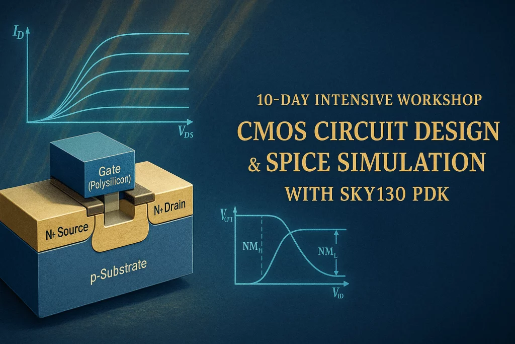
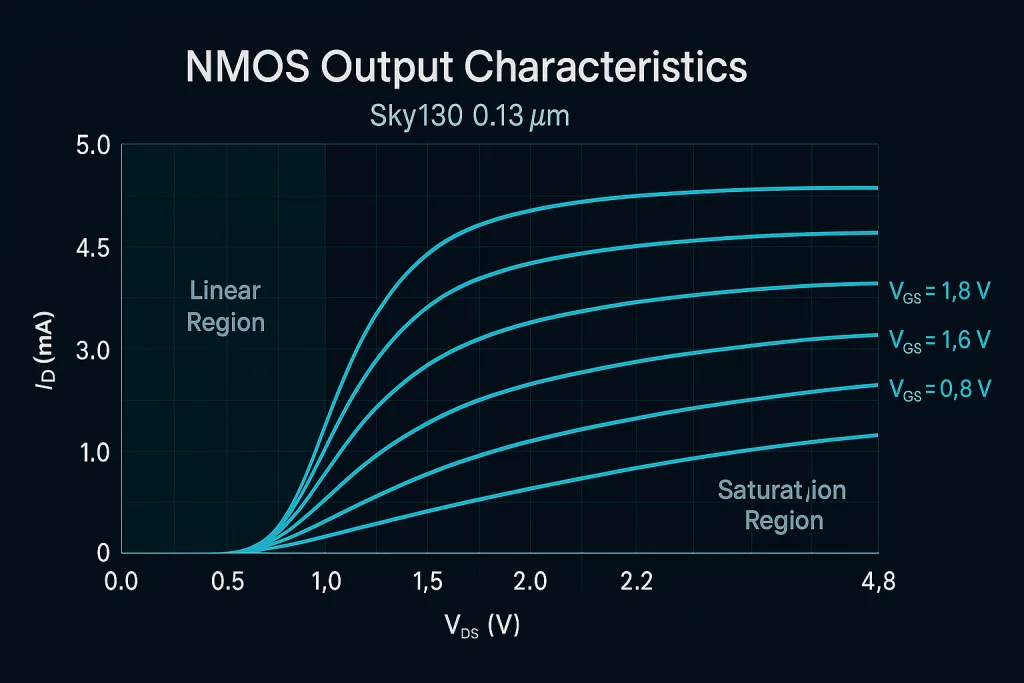
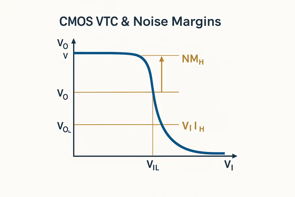
This workshop is designed to provide a deep understanding of CMOS design fundamentals through SPICE simulations. Over five days, participants will explore the behavior of NMOS and CMOS inverters in different operating regions, evaluate switching thresholds, noise margins, and analyze robustness against supply and device variations. Each session includes hands-on SPICE simulations backed by strong theoretical foundations, making it ideal for learners who wish to master transistor-level circuit behavior.
The global semiconductor resurgence – fueled by sovereign CHIPS initiatives, a surging demand for edge‑AI silicon, and an acute shortage of analog‑mixed‑signal talent – has made open, mature‑node platforms like SKY130 the fastest on‑ramp from idea to tape‑out. This ten‑day, cloud based online workshop positions you at the heart of that movement, translating industry‑grade CMOS theory into actionable design insight while leveraging the very PDK that start‑ups, national fabs, and university shuttle programs now rely on for first‑silicon success.
Across 10-days, you will dissect device physics, construct parameter‑swept SPICE decks, and benchmark inverter robustness under real‑world process and voltage variation. Each module pairs concise lectures with guided labs – covering velocity‑saturation, noise‑margin optimisation, dynamic power analysis, and script‑driven verification – so every concept is cemented by plots you generate yourself. Exclusive toolchains, reference designs, and daily design clinics ensure you leave with reusable IP blocks and a repeatable simulation workflow that dovetails directly into open‑source RTL‑to‑GDS flows such as OpenLane and VSDFlow.
Graduates emerge ready to contribute immediately to low‑power IoT nodes, automotive safety ICs, and chiplet‑based heterogenous packages – all markets leaning heavily on 130 nm for cost‑balanced innovation. Whether you aim to upskill a design team, strengthen research credentials, or fast‑track a prototype toward fabrication, this program delivers the simulation mastery and process‑aware mindset demanded by today’s accelerated semiconductor landscape.

Kunal Ghosh, the visionary co-founder of VLSI System Design (VSD) Corp. Pvt. Ltd., stands at the forefront of online open-source EDA and hardware design education, particularly in the realm of RISC-V.
With a portfolio of 50 top-tier VLSI online courses, Kunal has enriched the learning journey of over 90,000 students across 153 countries. His expertise extends beyond training; he’s actively involved in pioneering open-source projects and design collaborations with esteemed institutions like IIT Madras, IIT Bombay, IIT Guwahati and IIT Hyderabad.
His current focus is on crafting high-quality open-source Analog/Digital IPs, a groundbreaking endeavor in open-source hardware design. Kunal’s rich industry experience includes roles at Qualcomm and Cadence, specializing in SoC design. He holds a master’s degree from IIT Bombay, where he specialized in VLSI & Nano-electronics, with a focus on sub-100nm Electron Beam Lithography Optimization techniques.
Yes. The entire workshop runs on a cloud‑hosted platform, so you can log in whenever it suits you, watch the day’s lectures, complete the SPICE labs, and log out. Round‑the‑clock mentor support is available via WhatsApp, staffed by experts in multiple time zones throughout the ten‑day program.
Absolutely. Seasoned ASIC and SoC engineers regularly use this boot camp to renew transistor‑level intuition, benchmark SKY130 workflows, and adopt the latest open‑source methodologies. The material scales—letting veterans dive deeper into advanced sizing, PVT analysis, and low‑power optimisation while networking with peer professionals.
Yes. We start from first principles—introducing MOSFET physics, basic SPICE syntax, and step‑by‑step inverter design—before moving to advanced topics. Detailed lab guides and continuous mentor support ensure first‑time learners can follow along and succeed.
Workshop videos, notes, and netlist templates remain available for the full ten‑day window. Because this is an industry‑oriented, time‑boxed sprint, all graded lab submissions must be completed within those ten days to qualify for certification.
No. All simulations run on the VSD Virtual Desktop Infrastructure (VDI) that you’ll access on day one using a lightweight client. After the workshop, we provide scripts and templates so you can install the same toolchain on your personal system if desired.
Over the past five years, more than 1,000 engineers and students have completed this program and leveraged its CMOS‑gate foundations to excel in analog design, static‑timing analysis, and ECO roles at top semiconductor and EDA firms. Recruiters know the certificate signals job‑ready competence in circuit design and SPICE verification, making it a powerful credential for your résumé.
Cloud based Workshop
VSD, standing as a trailblazing Semiconductor EdTech company and a community-based Technology Aggregator, is revolutionizing the landscape of VLSI Design. With the belief that “Creativity is just connecting things”, VSD has mastered the art of linking the right resources with the community. This unique approach has sparked a significant transformation in the VLSI Design process.
Over the past decade, VSD has made remarkable strides in the open-source semiconductor domain. Our journey includes the development of comprehensive training content, empowering students to design silicon-grade IP/SoC. Notably, we’ve successfully guided these projects through the tapeout cycle via the Google open shuttle program. This achievement is a testament to our commitment to hands-on, practical education.
At VSD, our role extends beyond traditional education. While we didn’t invent EDA tools or design flows, we’ve made them accessible to a wider community. Our mentorship has been instrumental in the development of over 50+ Analog/Digital IPs and solutions. Impressively, 20+ of these have successfully transitioned from concept to Silicon – a clear indicator of our effective approach and the high quality of work produced under our guidance.
We pride ourselves on fostering a community-based revolution in the Semiconductor Industry. By democratizing access to advanced tools and knowledge, VSD is not just educating individuals; we are building a community of innovators poised to lead the next wave of advancements in the semiconductor sector. With VSD, the future of VLSI Design is not just being written; it’s being rewritten by a passionate and empowered community.
VSDSquadron was launched by Prof. V. Kamakoti, Director of IIT Madras
VSD Launches VSDSquadron In Collaboration With IIT Madras & DIR-V

Job Roles, Convergence With Embedded Systems, and Startups
VSD showcased at Semicon India 2023

VSDSquadron Educational board on Tamil News channel
5 Day Workshop on VLSI Design Flow using RISCV and EDA Tools
Karnataka VLSI roadshow at Sahyadri College, Mangalore
Welcome to Ethical RISC-V IoT Workshop
The “Ethical RISC-V IoT Workshop” at IIIT Bangalore, organized in collaboration with VSD, is a structured, educational competition aimed at exploring real-world challenges in IoT and embedded systems. Participants progress through three stages: building an application, injecting and managing faults, and enhancing application security. The event spans from May 9 to June 15, 2024, culminating in a showcase of top innovations and an award ceremony. This hands-on hackathon emphasizes learning, testing, and securing applications in a collaborative and competitive environment.
VSDSquadron, a cutting-edge development board based on the RISC-V architecture that is fully open-source. This board presents an exceptional opportunity for individuals to learn about RISC-V and VLSI chip design utilizing only open-source tools, starting from the RTL and extending all the way to the GDSII. The possibilities for learning and advancement with this technology are limitless.
Furthermore, the RISC-V chips on these boards should be open for VLSI chip design learning, allowing you to explore PNR, standard cells, and layout design. And guess what? vsdsquadron is the perfect solution for all your needs! With its comprehensive documentation and scalable labs, thousands of students can learn and grow together.
With VSD Hardware Design Program (VSD-HDP), you have the opportunity to push the boundaries of what exist in open source and establish the new benchmark for tomorrow.
It will leverage your degree in Electrical or Computer Engineering to work with
Sounds exciting to just get started with expert mentors, doesn’t it? But we are looking for the next generation of learners, inventors, rebels, risk takers, and pioneers.
“Spend your summer working in the future !!”
Outcomes of VSD Online Research IP Design Internship Program
VSD – Intelligent Assessment Technology (VSD-IAT) is expertly built training platform and is suited for designer requirements. Semiconductor companies understand the value of training automation and Engineer performance enhancement, and do not need to be convinced of the impact of a virtual platform for learning. VSD trainings are quick, relevant, and easy to access from any device at any time zone.
VSD is working towards creating innovative talent pool who are ready to develop design and products for the new tech world. VSD believes in “Learning by doing principle” , and always prepare the student to apply the knowledge learned in the workshops, webinars and courses. We always push our students to work on new designs, test it and work continuously till it becomes the best performing design. Any student who enrolls to VSD community starts working with small design and grows with us and develops a tapeout level design with complete honesty and dedication towards the Work !!
Check out VSD Interns Achievement!
Welcome to the World’s only online conference in Semiconductor Industry VSDOpen Conference. With enormous support and global presence of audience from different segments of industrial lobby and academia made a highly successful event. Evolution is change in the genetic makeup of a population over time, online conference is one kind evaluation everyone adapt soon.
VSD offers online course in complete spectrum of vlsi backend flow from RTL design, synthesis and Verification, SoC planning and design, Sign-off analysis, IP Design, CAD/EDA automation and basic UNIX/IT, Introduction to latest technology – RISC-V, Machine intelligence in EDA/CAD, VLSI Interview FAQ’s.
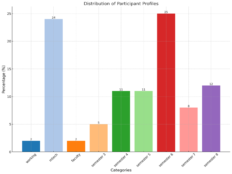
Current Reach – As of 2021, VSD and its partners have released 41 online VLSI courses and was successfully able to teach ~35900 Unique students around 151 countries in 47 different languages, through its unique info-graphical and technology mediated learning methods.
