Cloud Lab based Workshop
Bandgap IP Design using Sky130 technology node
Overview:
This course will be an in-depth introduction to Bandgap Reference (BGR) design and layout using open-source EDA tools (ngspice & Magic) and Google’s Skywater 130nm (SKY130) open-source process design kit (PDK). The course will focus on intuitive understating of the concepts involved in designing a BGR with real-world specifications and complete hands-on practice using the open-source EDA tools. During the 100 min course, the participant will start with the basic principles of BGR circuit, design, simulate and layout a complete industry-grade BGR – all of that in just 100 mins!
Day 1 – BGR Theory and Lab setup
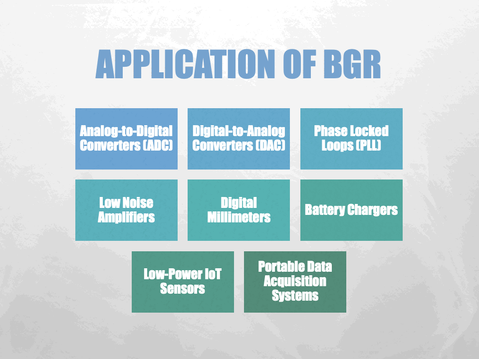
- Why temperature-independent voltage/current references for ICs
- Realization of BGR voltage reference.
- Circuit realization of a self-biased BGR and introduction to PTAT/CTAT current source
Day 2 – BGR Labs and post-layout simulations
- BGR components circuit simulations
- Steps to combine BGR sub-circuits and BGR full design simulation
- Post Layout simulations
- Steps to combine layouts
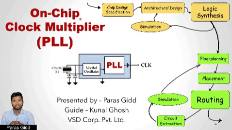
On-Chip Clock Multiplier (PLL) on OSU180.
Overview:
This course will be an in-depth introduction to On-Chip Clock Multiplier (PLL) design and layout using open-source EDA tools (ngspice & Magic) on OSU180nm. This course starts with fundamentals (from CMOS inverter & basic semiconductor physics) to Advanced IP design Process, issues & ways to deal with them (by live demo of entire IP from Design to Layout).
Anyone who finds VLSI interesting & want to start his/her journey on this wonderful path can find lamp posts laid out for you in a way you can build your own IP after attending this course sincerely.
- Introduction – Basics of IP, ASIC Design flow, On-chip clock Multiplier, PLL,
- Theory & fundamental Concepts – CMOS implementation, transistor sizing, 2nd order control system, IC fab process, Euler path.
- Pre-layout Implementation (lab session) – setting up system with linux, installation of tools, IP design, simulation & verification
- Post-layout Implementation (lab session) – device to block level layout, extracting parasitic capacitors, simulation & verification.
- Summary & Conclusion – Review Results, Future work, Acknowledgement.
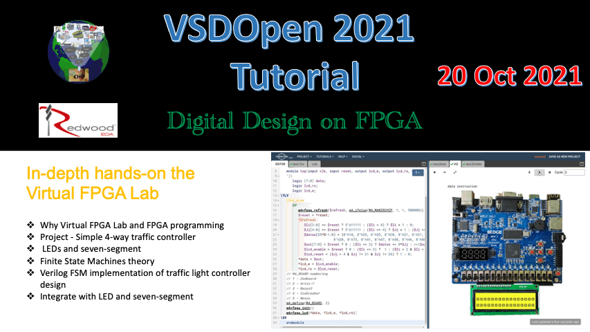
Digital Design on FPGA
Overview:
This course will be an in-depth hands-on demo session on the Virtual FPGA Lab using the open-source Makerchip IDE Web platform. The course will start with the introduction of why we need Virtual FPGA Lab and going through the Github repository. Then we will introduce the participants to Verilog. Theory is useful, but nothing beats practice!! We will design a 4-way traffic light controller using the concept of Finite State Machines in Verilog. We then visualize the output with LEDs and seven-segment displays in the Makerchip Virtual FPGA platform. Every part of this course has a theory followed by a lab.The student is required to have just a basic understanding of logic gates and no knowledge of the EDA tools is required.
Section 1: Makerchip and Virtual FPGA Lab theory and Lab Setup
- Motivation: Why Virtual FPGA Lab and FPGA programming
- Going through the GitHub repository
- About the project – Simple 4-way traffic controller – problem statement and end result
- Intro to LEDs and seven-segment – theory and lab
Section 2: 4-way traffic light controller design
- Introduction to Finite State Machines theory
- Verilog FSM implementation of traffic light controller design
- Integrate with LED and seven-segment
