Hello
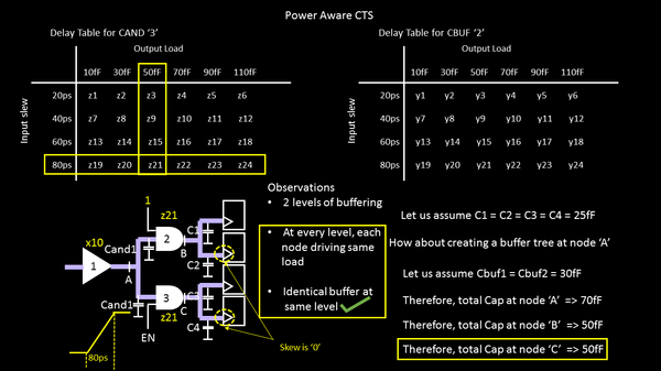
And here’s the solution to the problem posted in my previous article. ‘AND gate itself’. If you observe carefully, you tie one of the inputs of an AND gate to ‘logic 1’ and it will behave like a buffer. Advantage …. I will show you soon. Disadvantage… Area overhead

There are 2 advantages of using AND gate as buffer
1) you tend to use identical buffer at level 2 i.e. AND gate as buffer
2) you save power, by turning on/off the EN pin of AND gate 3 and disabling clock to whole bunch of flops connected to its output
3) you maintain zero skew while doing above 2.
Let’s take another valid scenario below, where both set of flops are active under certain conditions and conditions are driven by the values on the EN1 and EN2 pins

This is where again, we hit the scenario of non-zero skew due to different delay values of AND and OR gate for same set of input slew/output load conditions.

Let’s take the excitement to next post, where I will solve the above problem and also design a clock network, with above solutions, to see, in reality, how much power do we save.
“Learning should be a joy and full of excitement. It is life’s greatest adventure; it is an illustrated excursion into the minds of the noble and the learned” – Taylor Caldwell
Happy learning
Kunal
