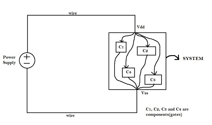
Concept of Decoupling Capacitors
A decoupling capacitor is a capacitor, which is used decouple the critical cells from main power supply, in order to protect the cells from the disturbance occurring in the power distribution lines and source. The purpose of using decoupling capacitors is to deliver current to the gates during switching. Herein, we would peep inside the reasons for the disturbance occurring in the power distribution lines. Observe the following figures.
If the wires were ideal, i.e. ‘zero’ resistance, ‘zero’ inductance and infinitely short, thus no issue of power distribution. To get the desired current during circuit operation, the source impedance should be minimal to do so.
Assume the ideal supply, and also include wire resistance and inductance in the figure below.
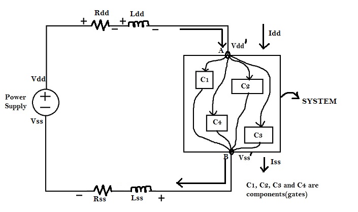
For time being consider capacitance to be zero for the discussion. Rdd, Rss, Ldd and Lss are well defined quantities. During switching operation, the circuit demands switching current i.e. peak current (Ipeak). Now, due to the presence of Rdd and Ldd, there will be a voltage drop across them and the voltage at Node ‘A’ would be Vdd’ instead of Vdd.
Vdd – Vdd’ = Ipeak*Rdd + Ldd * (dI/dt)
Similarly, same equation holds for (Vss’ – Vss) but current will be in opposite direction. Hence, now node A will observe a disturbance i.e. lowering of power supply voltage, commonly referred to as ‘voltage droop’. Also. Vss’, which is supposed to be at ‘zero’ potential, will be at some +ve potential, due to Rss and Lss. This is commonly referred to as ‘ground bounce’.
Now question is “What all can go wrong due to this distrubance?”
If the components were flip-flops, designed to operate at 1 V , and due to Rdd and Ldd, the voltage drops down to 0.6 V during switching, its possible that flip-flop doesnt function correctly.
And also logic ‘1’ would no longer be a logic ‘1’, since the circuit might have exceeded the noise margin. To understand this consider the following diagram :
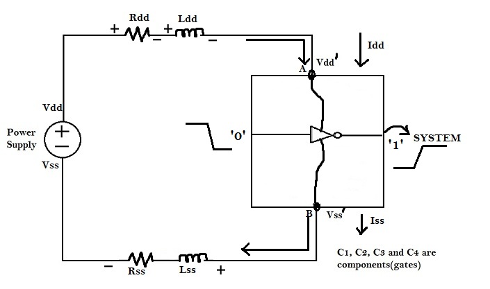
When input of the inverter switches from logic ‘1’ to logic ‘0’, output of inverter should switch from logic ‘0’ to logic ‘1’. This essentially means that the output capacitance of inverter should charge till the supply voltage Vdd’. But if Vdd’ goes below the noise margin, due to Rdd and Ldd, the logic ‘1’ at the output of inverter wont be detected as logic ‘1’ at the input of the circuit following the inverter.
Root cause of the problem is the disturbance occurring in the power supply line. As a system designer, you must assure three things
1) The noise injected is small enough that it doesn’t overcome the noise margin.
2) Local Power Supply should be healthy and create less disturbance in the performance of the Circuit.
Solution
1) Keep Rdd and Rss minimum by increasing width of wire.
2) Keep peak current Ipeak and change in current dI/dt as small as possible.
Ipeak = CL * Vdd / tr
dI/dt = CL * Vdd / tr2
Hence, limit the rise time (tr). If a circuit could run at 500 ps, its unnecessary to run the circuit at 300 ps. The largest possible value of tr should be selected.
From above equation, Ipeak and dI/dt also depends on load capacitance i.e. CL. Hence, reducing load, will also reduce Ipeak and dI/dt i.e. judicially decide the loading and the circuit components,as in turn it will not load the switching circuit.
3) Addition of Decoupling Capacitor in parallel with the circuit : The rise time and load capacitance could be controlled to reduce Ipeak, but limited upto certain level. Hence, an optimum solution is to connect a high value capacitor across the critical cell to the control the lowering of supply voltage . As this capacitor decouples the critical cells from main power supply it is called as decoupling capacitor. Refer to figure below
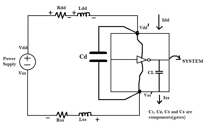
Every time the critical cell (in above diagram,an inverter) switches, it draws current to charge the load capacitor CL. This current consists of a both low and high frequency component. Most of the high frequency component, which is crucial part, is inserted by decoupling capacitor, whereas RL network replenish the charge (of CD) i.e. when the cell switches, it charges upto CLderived from CDstored in the decoupling capacitor, the RL network will charge the decoupling capacitor back to CD.
