X
"Join VSD-IAT cloud based Design Workshop on Sign-off Timing Analysis (STA) – Basics to Advanced"
Enroll Now
Skip to content
VLSI System Design Logo
  • Home
  • Products
    • Courses
    • VSD-IAT
    • VSD-Hardware Design Program
    • VSD-HDP Success Stories
    • VSD IP Specs
      • IP Specs
      • IP by Interns
    • VSD Tapeout
    • VSD Hackathon Series
    • VSD Library
    • Let Knowledge Win!!
  • Blogs
    • VSD latest Blogs
    • VSD (Initial phase)
    • VSD Video blog
  • VSDOpen
    • 2022
    • Collaboration Sponsor
    • 2021
    • 2020
    • 2019
    • 2018
  • About VSD
    • About us
    • Past Events
    • Upcoming Event…
    • Terms and Conditions
  • Explore

Tag Archives: p-type impurity doping

16-mask process – Looks complex.. not anymore!! – Part2

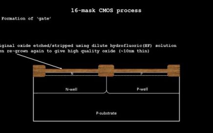
Hello ….continued from my previous post….. Once we have the nwell and pwell created, the entire structure is being placed in high temperature furnace and the […]

Continue reading

16-mask process – Looks complex.. not anymore!! – Part1

Hello If you look into the above image, and wondering how complex it is to build and package a chip, you will change your opinion […]

Continue reading

we are close… just wait ‘n’ watch!!

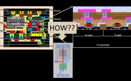
Hello Wondering…what are we closing on……!! So what if, I show you the below image which represents synthesized version some complex design (say, microprocessor)…you must […]

Continue reading

Blogs

© Copyright 2017 VLSI System Design Corporation
A SiteOrigin Theme
Facebook
Twitter
YouTube
YouTube
LinkedIn