Skip to content
VLSI System Design Logo
  • Home
  • Products
    • Courses
    • VSD – IAT
    • VSD IP Specs
      • IP Specs
      • IP by Interns
    • Tapeout
    • VSD Library
    • Design at $0
    • Let Knowledge Win!!
    • Workshop with EICT Academy IIT Guwahati
  • Blogs
    • VSD latest Blogs
    • VSD (Initial phase)
    • VSD Video blog
  • VSDOpen
    • 2020
    • Collaboration Sponsor
    • 2019
    • VSDOpen 2019 Keynote & Virtual Demo
    • 2018
    • VSDOpen 2018 Keynote & Paper
  • About VSD
    • About us
    • Past Events
    • Upcoming Event…
  • Explore

Tag Archives: drain region

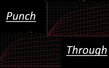
Let’s talk about currents – Punch through effect..

And it’s important, as this will set a back-ground for my upcoming new course on “CCS Timing Libraries”. So, in my last blog, we talked […]

Continue reading

Blogs

© Copyright 2017 VLSI System Design Corporation
A SiteOrigin Theme
Facebook
Twitter
YouTube
YouTube
LinkedIn
X
VSD aims to tackle global chip designer shortage
See how ?