VLSI is often introduced through disconnected terms: RTL, verification, synthesis, physical design, STA, DRC, LVS, tape-out and packaging. A fresher may recognise these words yet still struggle with the most important question:
How do all these activities connect to create a working semiconductor product?
The simplest answer is that chip development begins with a problem, moves through architecture and design, produces a manufacturable layout, and continues through fabrication, packaging, testing and board-level validation.
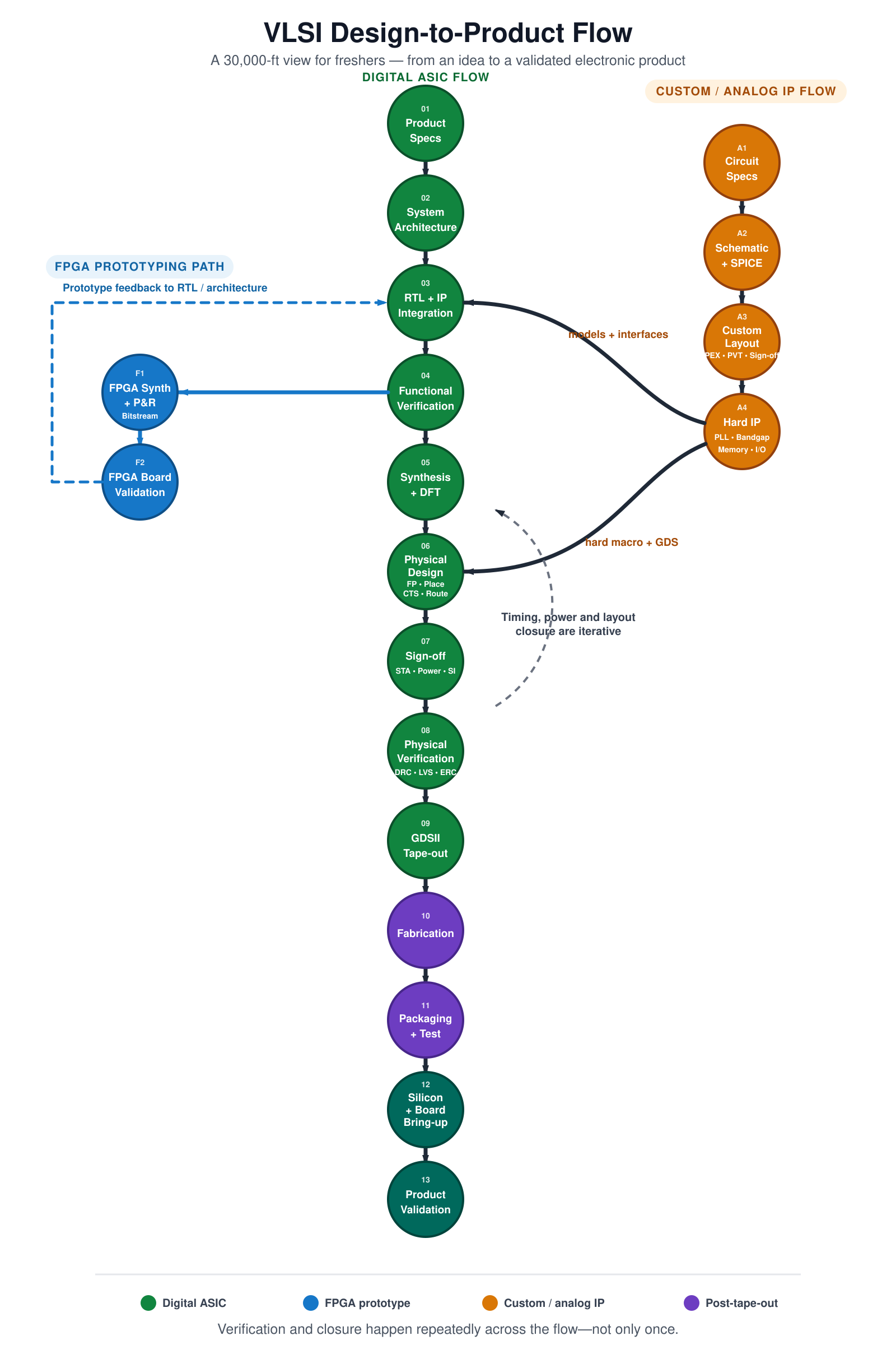
This article explains that journey from a 30,000-foot view. It also maps each stage to relevant programs on the VSD Learning Path, helping freshers choose a starting point that matches their interests.
Every chip begins with a problem—not with Verilog.
The specification defines the required functionality, performance, operating frequency, power budget, interfaces, memory, cost, area, reliability and intended application. For example, an edge-AI device may require sensor inputs, local inference, low power consumption and communication with an external host.
Input: A product or application requirement
Output: A measurable chip specification
VSD does not currently list a dedicated product-specification course. However, the application-to-processor relationship becomes clearer through the RISC-V based MYTH workshop and the Product-Based RISC-V Skilling Program.
The important lesson for a fresher is simple: RTL is an implementation of a specification. It is not the starting point of the product.
Architecture divides the specification into major subsystems such as processors, memories, buses, accelerators, peripherals, clocking, reset and analog interfaces.
Microarchitecture goes one level deeper. It defines how a processor or hardware block will implement that architecture through datapaths, control logic, pipelines, registers, ALUs and memory interfaces.
Input: Product specification
Output: Block diagram, interfaces and microarchitecture
For processor architecture, start with RISC-V based MYTH. It connects the RISC-V ISA to a basic and then pipelined CPU microarchitecture. Learners seeking deeper exposure to processor functionality, Verilog implementation, I/O and low-level C/assembly can continue with the Product-Based RISC-V Skilling Program.
Register-transfer level, or RTL, describes how data moves between registers and how combinational and sequential logic transforms it. Verilog or another hardware description language is used to implement counters, controllers, interfaces, processors and other digital blocks.
An SoC is rarely written entirely from scratch. Designers integrate reusable IP such as processor cores, memories, GPIO, UART, SPI, timers, PLLs and analog blocks. Every IP must have clearly defined clocks, resets, interfaces and timing expectations.
Input: Architecture and block-level specifications
Output: Synthesizable RTL and an integrated SoC design
A learner with little or no Verilog experience should begin with Master RTL Design and Synthesis. It covers RTL coding, simulation, testbenches, debugging and Yosys synthesis using SKY130 standard cells.
After learning basic RTL, RISC-V based MYTH provides a meaningful processor project, while the VSD Hardware Design Program expands the journey towards a complete RTL-to-GDSII implementation.
Before implementation, the RTL must be checked against the specification. Verification teams build testbenches, generate stimulus, inspect waveforms, write assertions and test normal, corner and error conditions.
Verification is not a single box that is completed once. It begins with individual blocks, continues at subsystem and SoC level, and reappears after synthesis and physical design through gate-level and post-layout checks.
Input: RTL and verification plan
Output: Functionally validated RTL, test results and bug reports
Master RTL Design and Synthesis introduces simulation, waveform debugging and testbench development. RISC-V based MYTH applies basic verification to processor design. The VSD Hardware Design Program adds pre-synthesis, post-synthesis and gate-level comparisons.
Freshers should note that the current VSD product page does not show a dedicated UVM, formal-verification or assertion-based verification program. These are natural advanced topics after mastering RTL and basic testbench development.
Verified RTL can be implemented on an FPGA. The FPGA flow performs synthesis, mapping, placement, routing and bitstream generation. The bitstream configures programmable logic so the design can run on real hardware.
FPGA prototyping allows designers to test interfaces, firmware and system behaviour before committing to the cost and time of ASIC fabrication. Problems discovered on the board can feed back into the architecture or RTL.
Input: Verified RTL
Output: FPGA bitstream and hardware validation results
The FPGA Fabric Design and Architecture Workshop explains LUTs, CLBs, switch boxes, routing and FPGA fabric construction. Learners ready to build processor peripherals and reusable IP can continue with the RISC-V FPGA IP Internship.
This is an optional branch in an ASIC project, but it is extremely valuable for processor, embedded-system and product-oriented designs.
Logic synthesis converts RTL into a gate-level netlist using standard cells from a technology library. The synthesis tool optimises the design for timing, power and area while respecting design constraints.
Design for test, or DFT, adds structures such as scan chains and test access logic so manufacturing defects can be detected after fabrication.
Input: Verified RTL, timing constraints and standard-cell libraries
Output: Optimised gate-level netlist and test-ready design
Master RTL Design and Synthesis is the most direct beginner program for understanding RTL-to-gate conversion. The VSD Hardware Design Program covers synthesis, constraints, optimisation and post-synthesis analysis. The SoC Design and Implementation Program uses Synopsys Design Compiler for industry-tool exposure.
The current VSD catalogue does not list a dedicated DFT/ATPG program, so learners should treat DFT as a specialised continuation after synthesis fundamentals.
A gate-level netlist describes connectivity but does not specify where cells and wires will physically exist on silicon. Physical design converts the netlist into a manufacturable layout.
The principal stages are:
Input: Synthesised netlist, constraints, libraries and PDK
Output: Placed-and-routed physical database
The strongest entry point is Digital VLSI SoC Design and Planning, which introduces floorplanning, standard cells, timing and the OpenLANE RTL-to-GDSII flow.
For deeper project work, learners can choose the VSD Hardware Design Program, the VSDSquadron RTL-to-GDS Program, or the SoC Design and Implementation Program using Synopsys tools.
Although Digital VLSI SoC Design and Planning is listed as a starter course, it technically maps to the physical-design and sign-off portion of the chip flow. A complete beginner will understand it better after gaining basic RTL and synthesis knowledge.
A routed layout is not ready for manufacturing merely because every connection exists. Engineers must prove that the design works across process, voltage and temperature conditions.
Sign-off activities include:
Input: Routed layout, parasitics and timing libraries
Output: Sign-off reports and a timing/power-clean design
Digital VLSI SoC Design and Planning introduces timing analysis using OpenSTA. The VSD Hardware Design Program performs STA after synthesis, placement, CTS and routing. For commercial-tool exposure, the SoC Design and Implementation Program uses PrimeTime and StarRC.
Timing closure is iterative. Violations may require changes to constraints, synthesis, placement, clock trees or routing.
Physical verification checks whether the final layout can be manufactured and whether it still represents the intended circuit.
Important checks include:
Input: Final layout and foundry rule decks
Output: DRC/LVS/ERC-clean, tape-out-ready GDSII
The most direct program is Physical Verification for Tapeout Readiness using SKY130. It covers DRC, LVS, extraction, antenna, density, hierarchy, macros and GDS sign-off using open-source tools. The SoC Design and Implementation Program also introduces physical verification through Synopsys IC Validator.
After sign-off, the final GDSII database and supporting information are submitted for tape-out. The foundry uses this data to generate masks and fabricate wafers through repeated deposition, lithography, etching, implantation and metallisation processes.
Input: Signed-off GDSII and tape-out package
Output: Fabricated wafers containing the designed dies
The VSD Tapeout initiatives provide the closest connection to this stage. Physical Verification and RTL-to-GDSII programs prepare learners for tape-out, but semiconductor fabrication itself is a specialised foundry discipline and is not currently presented as a standalone VSD course.
Fabricated dies must be separated from the wafer, assembled into packages, connected to package pins or bumps, protected and tested.
Packaging affects electrical performance, thermal behaviour, mechanical reliability, signal integrity, power delivery and system cost. Modern options include wire-bond packages, flip-chip, wafer-level packaging, chiplets and 2.5D/3D integration.
Input: Fabricated and tested dies
Output: Packaged semiconductor devices ready for system use
The Packaging Fundamentals of Design and Testing workshop covers package selection, assembly, thermal simulation, reliability, testing, wire bonding, flip-chip and advanced packaging concepts.
After packaging, engineers place the device on a PCB and power it on. They verify clocks, reset, power rails, JTAG, memories, peripherals, firmware and external interfaces.
This stage reveals problems that simulation may not have exposed. The team compares real measurements against pre-silicon expectations, diagnoses failures and qualifies the system across operating conditions.
Input: Packaged chip, PCB, firmware and test plan
Output: Working silicon, board-level evidence and characterised performance
The RISC-V Embedded Firmware Internship and VSDSquadron hardware platform help learners understand the relationship between processors, firmware, interfaces and physical hardware.
A successful chip is not automatically a successful product. The final system must solve its target problem reliably, repeatedly and within power, performance and cost limits.
Product validation may include application workloads, AI-model deployment, sensor testing, communications, environmental testing, security, firmware updates and long-duration reliability checks.
Input: Working silicon and board
Output: A validated electronic product or demonstrator
Learners interested in connecting RISC-V hardware to real AI workloads can explore the RISC-V EdgeAI Workshop and the RISC-V Edge AI Internship.
Digital RTL is only one part of a modern SoC. Chips also require transistor-level blocks such as PLLs, bandgaps, ADCs, DACs, SRAMs, I/O cells and power-management circuits.
The custom-IP flow generally follows:
Circuit specification → schematic → SPICE simulation → device sizing → PVT analysis → custom layout → extraction → post-layout simulation → IP sign-off → SoC integration
Start with CMOS Circuit Design and SPICE Simulation using SKY130 to understand MOSFET behaviour, CMOS inverters, noise margins, delay, power and PVT variation.
Continue with Bandgap IP Design using SKY130 to design and characterise a real analog reference block. Learners interested in advanced transistor technology can then explore FinFET Circuit Design and Characterization.
The completed analog IP supplies behavioural models and interfaces for SoC verification, timing/power models for design tools, and physical abstracts or GDS for physical integration.
There is no single first course for everyone. The correct starting point depends on the role you want to explore.
CMOS Circuit Design and SPICE Simulation → Bandgap IP Design → Physical Verification → Analog/Mixed-Signal IP project or internship
RISC-V MYTH → Product-Based RISC-V Skilling → Embedded/FPGA hardware project → RISC-V EdgeAI → RISC-V Edge AI Internship
The semiconductor journey does not end when RTL simulates correctly. It does not end when synthesis produces a netlist, when physical design produces GDSII, or even when a chip is fabricated.
A complete electronic-product journey is:
Problem → Specification → Architecture → RTL/IP → Verification → Prototype → Synthesis → Physical Design → Sign-off → Physical Verification → Tape-out → Fabrication → Packaging and Test → Board Bring-up → Product Validation
Freshers do not need to master every stage immediately. They need to understand the complete map, select one entry point and build evidence through labs, reports, GitHub repositories, hardware demonstrations and progressively larger projects.
That is how isolated VLSI topics become a coherent semiconductor career journey.
Explore the complete collection of courses, workshops, boards and internships on the VSD Products and Learning Path page.
Welcome to Ethical RISC-V IoT Workshop
The “Ethical RISC-V IoT Workshop” at IIIT Bangalore, organized in collaboration with VSD, is a structured, educational competition aimed at exploring real-world challenges in IoT and embedded systems. Participants progress through three stages: building an application, injecting and managing faults, and enhancing application security. The event spans from May 9 to June 15, 2024, culminating in a showcase of top innovations and an award ceremony. This hands-on hackathon emphasizes learning, testing, and securing applications in a collaborative and competitive environment.
VSDSquadron, a cutting-edge development board based on the RISC-V architecture that is fully open-source. This board presents an exceptional opportunity for individuals to learn about RISC-V and VLSI chip design utilizing only open-source tools, starting from the RTL and extending all the way to the GDSII. The possibilities for learning and advancement with this technology are limitless.
Furthermore, the RISC-V chips on these boards should be open for VLSI chip design learning, allowing you to explore PNR, standard cells, and layout design. And guess what? vsdsquadron is the perfect solution for all your needs! With its comprehensive documentation and scalable labs, thousands of students can learn and grow together.
With VSD Hardware Design Program (VSD-HDP), you have the opportunity to push the boundaries of what exist in open source and establish the new benchmark for tomorrow.
It will leverage your degree in Electrical or Computer Engineering to work with
Sounds exciting to just get started with expert mentors, doesn’t it? But we are looking for the next generation of learners, inventors, rebels, risk takers, and pioneers.
“Spend your summer working in the future !!”
Outcomes of VSD Online Research IP Design Internship Program
VSD – Intelligent Assessment Technology (VSD-IAT) is expertly built training platform and is suited for designer requirements. Semiconductor companies understand the value of training automation and Engineer performance enhancement, and do not need to be convinced of the impact of a virtual platform for learning. VSD trainings are quick, relevant, and easy to access from any device at any time zone.
VSD is working towards creating innovative talent pool who are ready to develop design and products for the new tech world. VSD believes in “Learning by doing principle” , and always prepare the student to apply the knowledge learned in the workshops, webinars and courses. We always push our students to work on new designs, test it and work continuously till it becomes the best performing design. Any student who enrolls to VSD community starts working with small design and grows with us and develops a tapeout level design with complete honesty and dedication towards the Work !!
Check out VSD Interns Achievement!
Welcome to the World’s only online conference in Semiconductor Industry VSDOpen Conference. With enormous support and global presence of audience from different segments of industrial lobby and academia made a highly successful event. Evolution is change in the genetic makeup of a population over time, online conference is one kind evaluation everyone adapt soon.
VSD offers online course in complete spectrum of vlsi backend flow from RTL design, synthesis and Verification, SoC planning and design, Sign-off analysis, IP Design, CAD/EDA automation and basic UNIX/IT, Introduction to latest technology – RISC-V, Machine intelligence in EDA/CAD, VLSI Interview FAQ’s.
Current Reach – As of 2021, VSD and its partners have released 41 online VLSI courses and was successfully able to teach ~35900 Unique students around 151 countries in 47 different languages, through its unique info-graphical and technology mediated learning methods.