I have been tracking opensource tools in backend flow and also VSD’s online programs like MYTH, Digital System Design, Modelling using Verilog etc. In the meanwhile, I have been taking training on backend so I was very much curious to explore available tool part by mapping to the conventional EDA tools. That’s when I decided to join “Advanced Physical Design using OpenLANE/Sky130” which happened in the month of April, 2021.
I will walk through my journey where I will be mapping the traditional ASIC back-end flow with the OpenLANE flow. At the end, I will showing be a flowchart in OpenLANE flow as well as available tools for each step in the back-end flow, in the present EDA market.
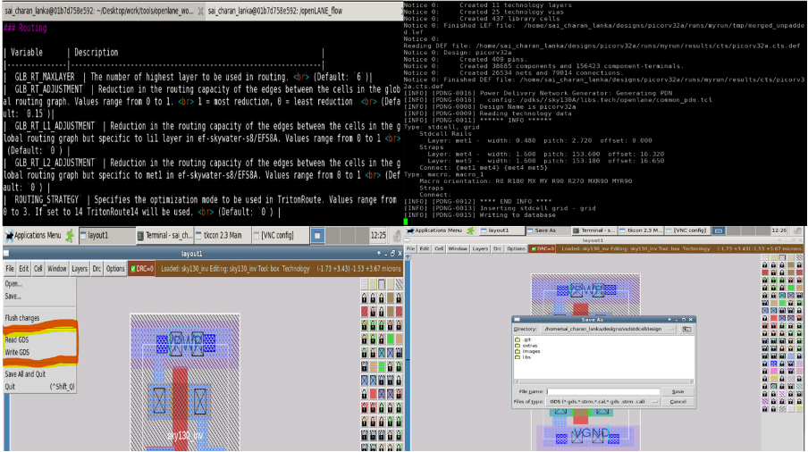
Before we start with the standard steps, we need to prepare the OpenLANE flow by providing the respective Verilog, .lib and .lef file locations in a script called “config.tcl”. Once we evoke the Openlane using the “flow.tcl” script, all tools will be setup with default configurations. Once we envoke the flow under ‘interactive mode’, we need to prepare it with the required design name and the database folder in which all our results, logs, errors will be stored, for that current run of the flow. Once we complete it, we will be proceeding with the actual steps same as that of ASIC flow.
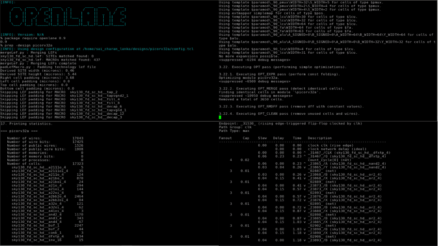
Step 1 - Synthesis:
- ASIC flow
- Running synthesis by providing liberty files, Verilog files, sdc files.
- Mapping of gates to library gates.
- Optimizing the design
- OpenLANE flow
- Since we already mentioned the files list and other default configurations in the scripts, we just use run_synthesis command to perform synthesis.
- After this, the abc tool maps the gates and the optimizes the netlist generated
- Immediately, OpenSTA tool gets invoked to perform the timing analysis and output the timing report.
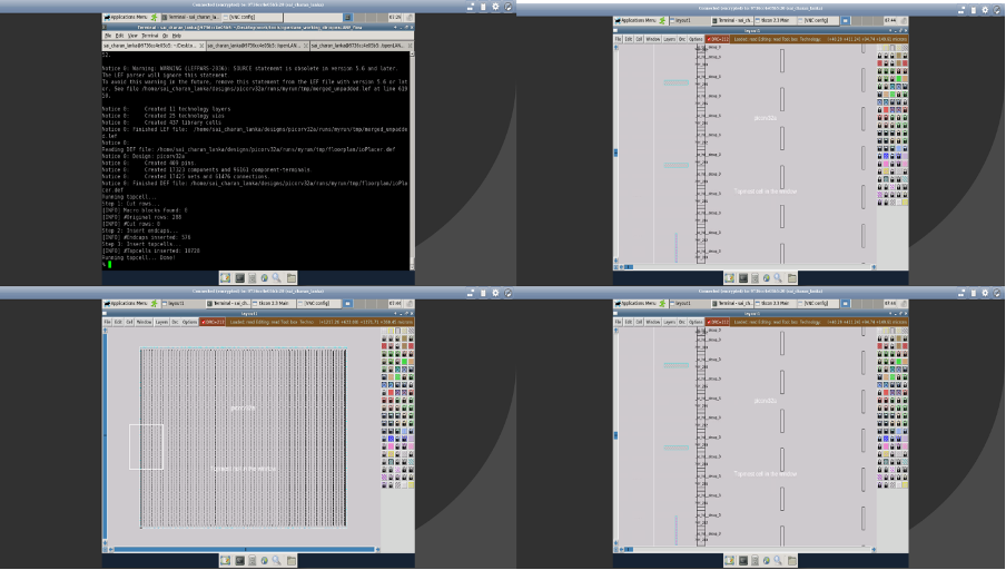
Step 2 - Floorplanning
- ASIC flow
- Provide die and core utilization ratios, aspect ratio
- Pin placement
- Power planning
- Placement of physical cells
- Placing of blockages
- OpenLANE flow
- Die and core utilization ratios, aspect ratio are set to default in the configs file. We just need to use run_floorplan command to perform floorplanning
- IO pins are placed automatically
- Physical cells are placed automatically
- Blockages are added
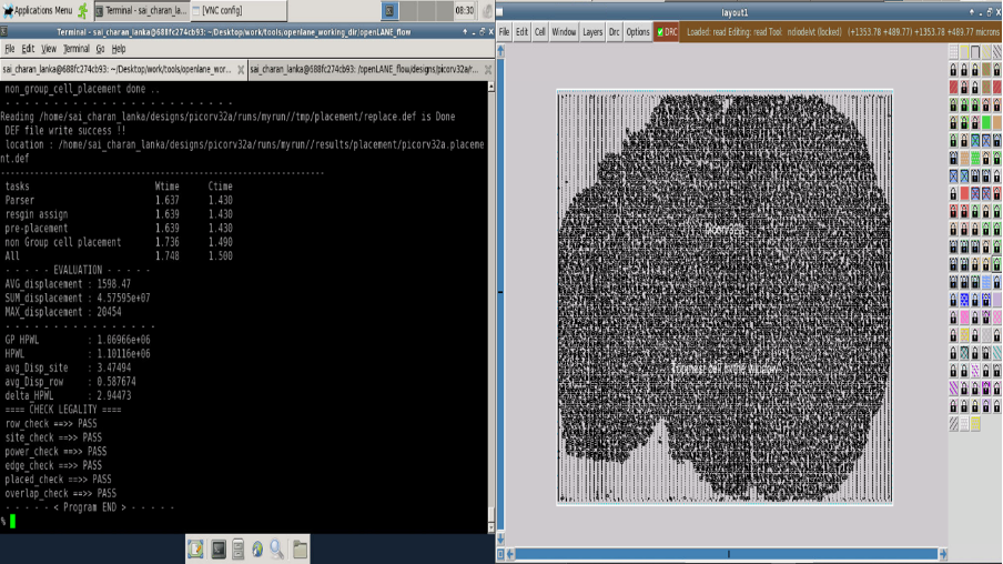
Step 3 - Placement
- ASIC flow
- Placement is done in two stages: Global placement, legalizing locations and detailed placement
- OpenLANE flow
- Placement is done using a command run_placement. Similar to ASIC flow, placement is done stages – Global placement, Detailed placement and optimization.
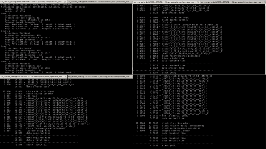
Step 4 - CTS
- ASIC flow
- Creating a specs file containing NDR rules, clock buffer and inverter types etc.
- CTS engine creates the clock network for the design by following hybrid algorithms.
- OpenLANE flow
- CTS stage is done using run_cts command.
- All CTS specific cells are set in the config file.
Step 5 - Routing
- ASIC flow
- Post-checking of timing reports for violations, we proceed to routing stage.
- This will be the last part of PnR flow after which DRC and connectivity violations are verified.
- OpenLANE flow
- First, power distribution network is created. We do it by using a command - gen_pdn.
- Then, we proceed to actual routing. Same like in ASIC flow, routing is done in two stages – global routing and detailed routing. We do it by using a command run_routing. This will also extract spef file.
Step 6 - RC Extraction
- ASIC flow
- Spef files are extracted using specific commands after the routing stage. In the spef file we get the information of parasitics which will be helpful in finding and clearing timing violations. We migrate between tools to do these checks.
- OpenLANE flow
- We can extract the spef separately using SPEF EXTRACTOR tool.
Step 7 - Physical Verification and GDSII
- ASIC flow
- We check for manufacturing issues like DRC, LVS, ERC etc., using foundry given rule decks. Once we get the drc-clean design, we extract the gdsii file for manufacturing the chip.
- OpenLANE flow
- We can run these checks in the flow itself using commands run_magic_drc, run_lvs. Once we are confident with our clean design, the gdsii file is extracted using run_magic. This is the final step after which the design in the form of GDSII format is sent for manufacturing.
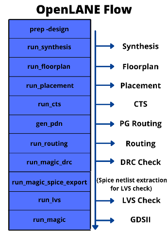
Below is the flowchart showing the list of commands used in OpenLANE flow used at different stages in the back-end flow.
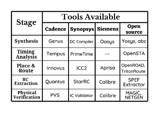
Below is the table comparing tools available in market including opensource for back-end flow.
 In the workshop, I experienced the opensource environment in backend flow, embedded a custom standard cell in the main design and tested the complete flow. This freedom of building a chip, no matter who we are, is revolutionary.
Limitations of Opensource environment:
- MMMC (Multi Mode Multi Corner) not supported yet
- Noise characterization not supported yet
- PDKs available for technologies 130nm (Sky130 PDK) which is far away from the current technology (in 5nm, 7nm)
But for designs working in low frequencies and in single modes, opensource tools can serve the purpose of developing them and getting benefitted by this OpenLANE using its “no human interaction” advantage.
In the end, for the question “What I did in the 5-day Advanced Physical Design using OpenLANE/Sky130 workshop?”, the answer is “I experienced an immense freedom within expanding boundaries”
