Semiconductor memories are an integral part of all systems to store large quantities of digital information. One of the important types of semiconductor memory is Static Random-Access Memory which is mainly used as memory caches and processor registers.
Why OpenRAM?
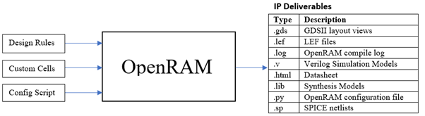
OpenRAM is an open-source technology independent memory compiler which generates fabricable SRAM design. Its SRAM architecture consists of bit cell array with peripherals like address decoder, the word line drivers, the column multiplexer, the precharge circuitry, the sense amplifier, the write drivers and the control logic. It requires custom cells like bitcell, sense amplifier, write drivers, tristate buffers and D-flip flop for each technology added to it. For OSU 180 nm SRAM IP, all the custom cells are designed and simulated using open-source EDA tools like ngspice and MAGIC VLSI layout tool. It uses the technology files, custom cells designed and configuration script to generate SPICE netlists, layout, timing and power models and other IP deliverables required for fabricating SRAM as shown in the above figure.
Custom Cell Design
- 6T Cell
Schematic
 Layout
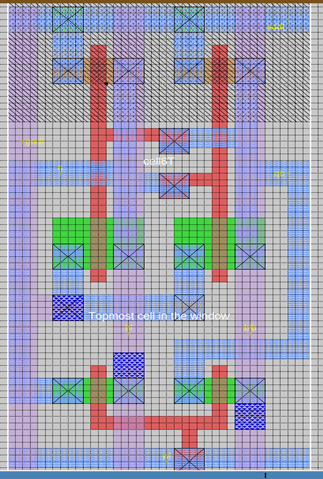
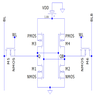
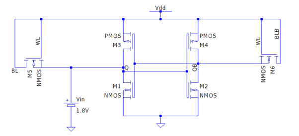
It uses bistable cross-connected inverters (M1, M3 & M2, M4) as a latching circuit. Based on the state of the latch circuit the data is interpreted as logic ‘1’ or ‘0’. The access switches M5 & M6
(NMOS pass transistors) are used to connect the bit line (column selection signal) to the cell to read or write data and are controlled by the word line (WL). The bit line BL & BLB will always have complementary values due to the inverting functionality of the feedback loop which helps in determining the stored data value. The cell ratio (CR) and pull-up ratio (PR) used is 2 & 1 respectively.
Read Operation: Whenever the word line is activated, the data at the internal nodes Q & QB appear at the bitlines BL & BLB respectively.
Prelayout Simulation
Postlayout Simulation
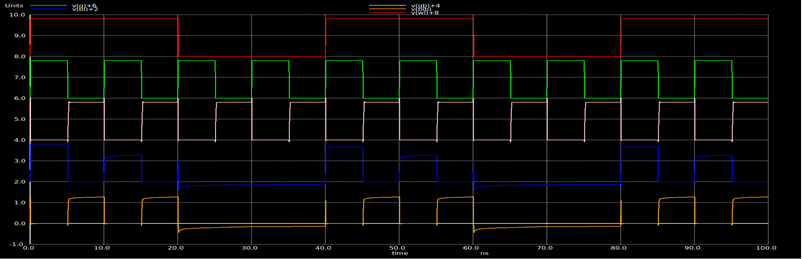
Write Operation: Whenever the word line is activated, the data present at the bitlines BL & BLB is written at the internal nodes Q & QB respectively.
Postlayout Simulation
Cell Stability Analysis
- SNM Analysis
The stability and writability of the cell are quantified by the hold margin, read margin and write margin which are determined by the static noise margin (SNM). It determines how much noise can be applied at the inputs of the two cross coupled inverters before a stable state is lost during hold or read operating mode or a second stable state is created during write operation.
Hold SNM: In hold SNM analysis, the inverters are separately analyzed and the access transistors are disconnected from the inverters as shown above. SNM curve (butterfly curve) is obtained by plotting VTC of one inverter with the inverse VTC of another inverter as shown below.
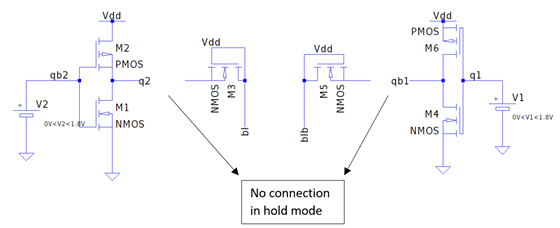
Setup for extracting hold SNM
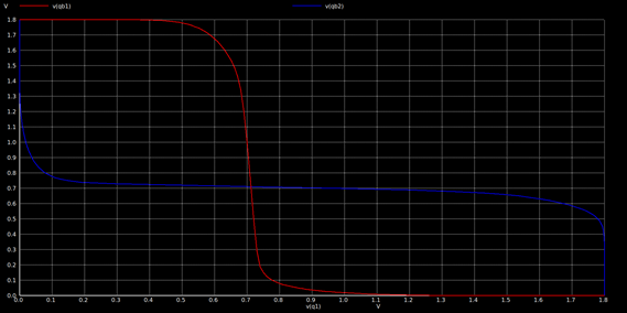
Hold SNM Curve
By fitting the largest square in the upper and lower loops, we get SNMH = 0.91V and SNML = 0.61V respectively. Hold SNM = min (SNMH, SNML) = 0.61V
Read SNM: Read SNM curve is obtained by performing similar steps as in hold SNM except that the access transistors are connected to the inverters.
Setup for extracting Read SNM
Read SNM Curve
Read SNM = min (SNMH, SNML) = min (0.48,0.39) = 0.39V
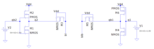
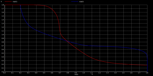
Write SNM: In Write SNM analysis, a write ‘0’ operation is used by connecting BL to the ground potential. Write SNM curve is obtained by plotting the write VTC of the first inverter and the read VTC of the second inverter together.
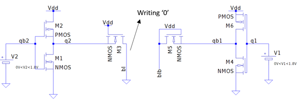
Setup for extracting Write SNM
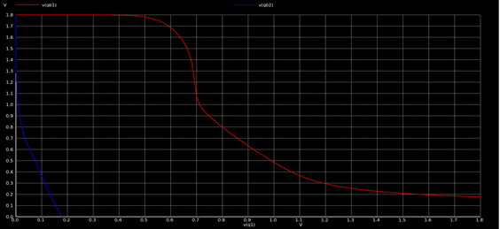
Write SNM Curve
By fitting the smallest square between the two curves, we get Write SNM = 1.063V
- N-Curve
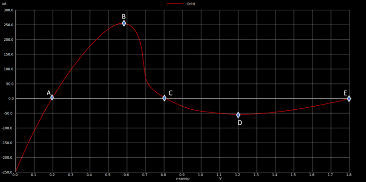
N-curve provides the current flow information along with the voltage metrics which is equally important for an overall analysis of cell stability. For obtaining the N-curve, BL, BLB & WL are connected to Vdd and a voltage source is applied at either of the internal nodes Q or QB and then the current entering that node is plotted against the input voltage.
Setup for N-curve
N-curve
Read Stability Metrics
Static Voltage Noise Margin (SVNM) – It is the maximum tolerable dc noise voltage at internal nodes of the bitcell before its content flips and it is measured as the difference between point C and point A. SVNM = 0.617V
Static Current Noise Margin (SINM) – It is the maximum tolerable dc noise current injected at internal nodes of the bitcell before its content changes and it is denoted by point B. SINM = 255.67uA
Write Stability Metrics
Write Trip Voltage (WTV) – It is the minimum voltage drop needed to change the internal nodes of the bitcell and it is measured as the difference between point E and point C. WTV = 0.988V
Write Trip Current (WTI) – It is the minimum amount of current needed to write the bitcell and it denoted by point D. WTI = -53.47uA
2.Sense Amplifier
Schematic
 Layout
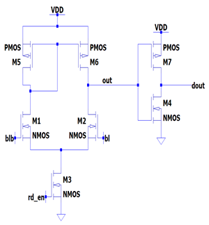
A sense amplifier senses a small voltage difference at its inputs BL & BLB and amplifies it to a recognizable logic ‘0’ or ‘1’ voltage level at the output terminal dout. With the help of the sense amplifier, the data read operation is performed at a faster rate thereby increasing the access time.
Prelayout Simulation
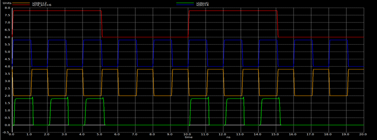
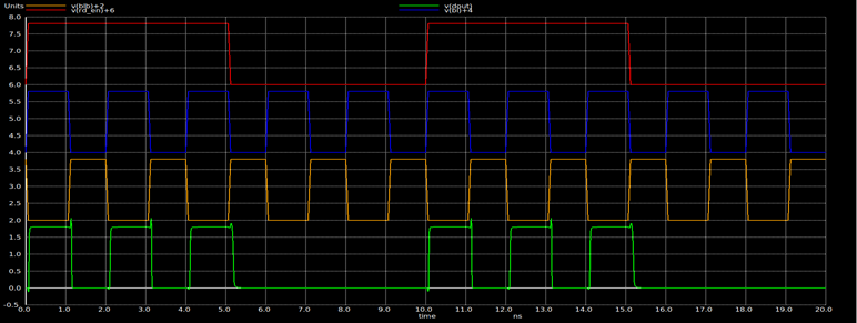
3.Write Driver
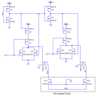
Schematic 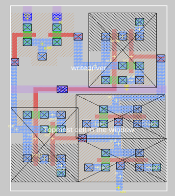
Layout
The above figure shows the data write circuitry for sram. Whenever wb goes low, the input data is written to the bitlines BL & BLB. The precharge circuit keeps the bitlines to Vdd when no read or write operation is performed. If din=0 (or 1) then the bitline BL (or BLB) discharges through the nmos transistor.
Prelayout Simulation
Postlayout Simulation
4. Tristate Buffer
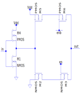
Schematic
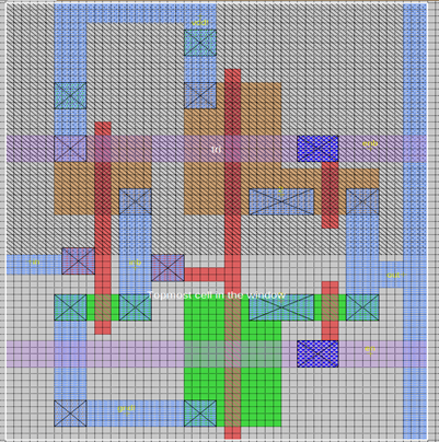 Layout
A tristate buffer allows multiple logic blocks to be connected to the same line without damage or loss of data. The above tristate buffer uses a differential enable signal. Whenever enable signal is present the input data is present at the output otherwise output remains in high impedance state.
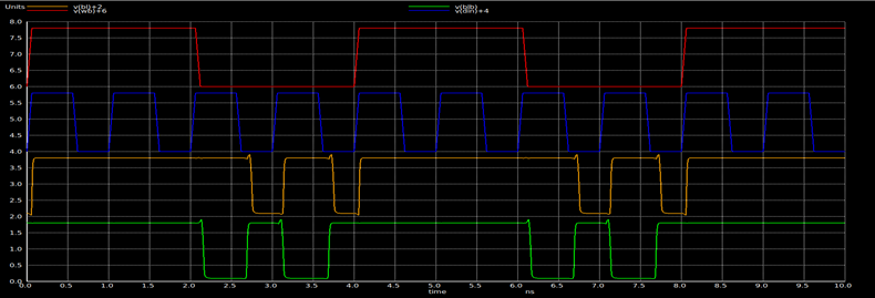
Prelayout Simulation
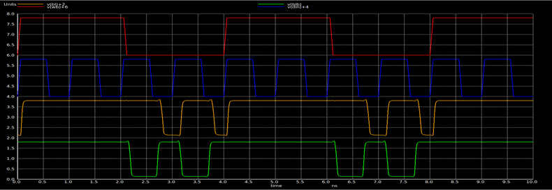
Postlayout Simulation
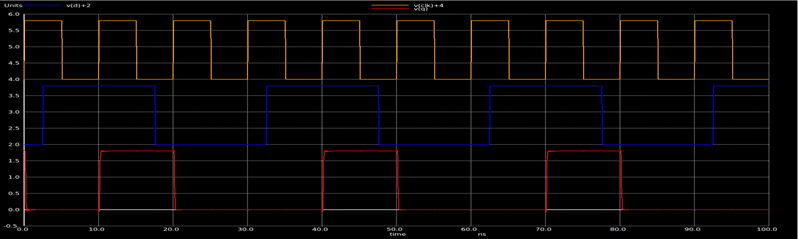
5. Positive Edge Triggered D-Flip Flop
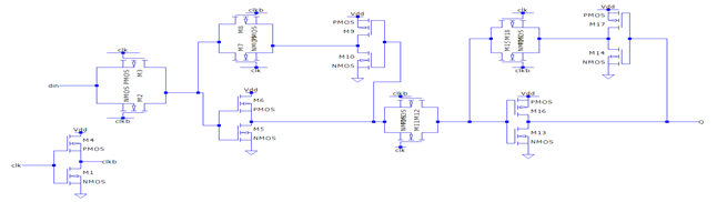
Schematic
In the above circuit, master-slave DFF is implemented. When the clock signal is low, the master latches the input data whereas slave retains the previous state. When the clk signal goes from low to high, the master is disconnected from the input and drives the slave thereby passing the input data at the output Q. DFF in SRAM is used as buffers.
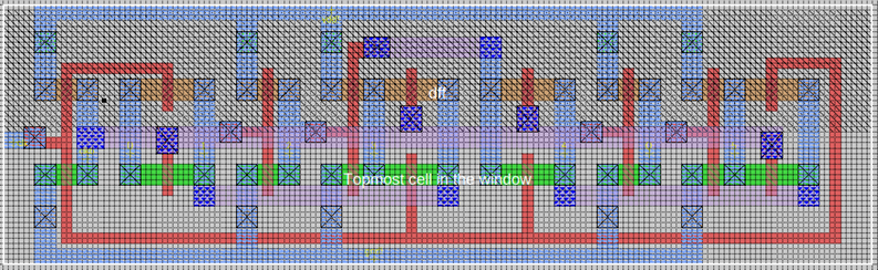
Layout
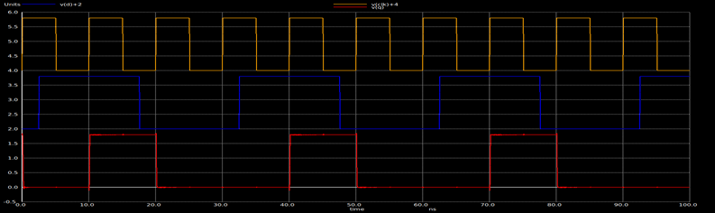
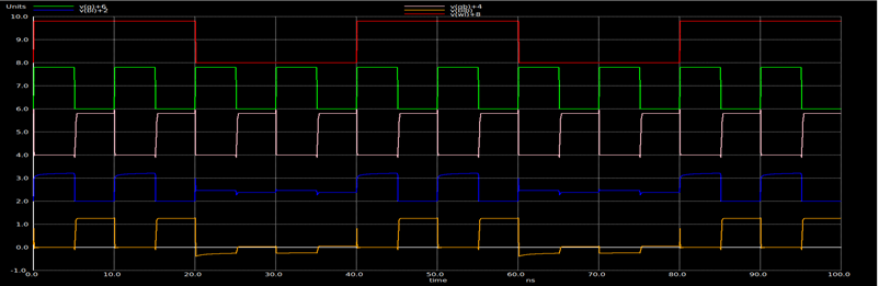
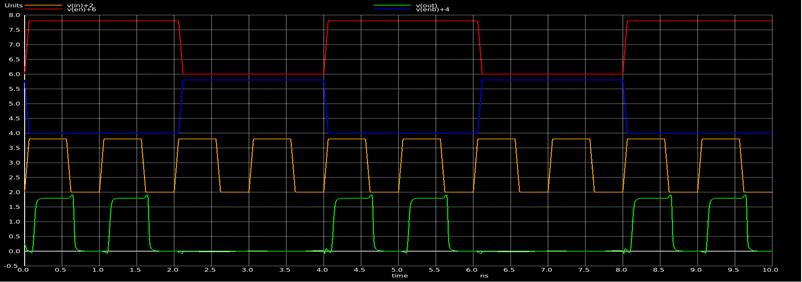
Prelayout Simulation
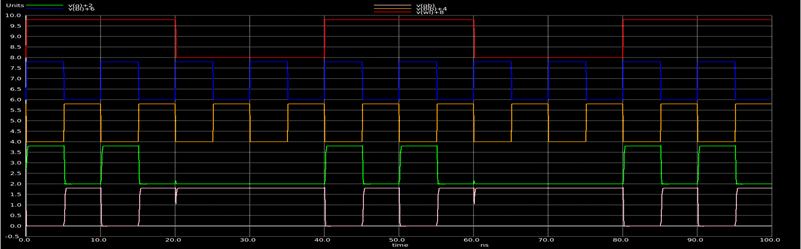
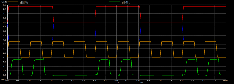
Prelayout Simulation
The below figure shows the OpenRAM compiler output which uses the above made cells for OSU180nm technology. However, the layout generated is not DRC clean because the compiler is not yet compatible with OSU180nm tech since it has not cleared compiler’s all internal regression test
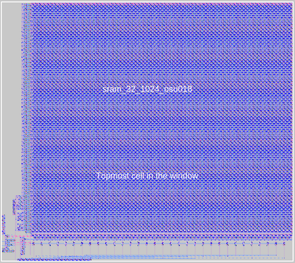
1024*32 (4kB) SRAM
Here is the GitHub link for this project: https://github.com/yash-k99/vsdsram
![]()
Refer below link to know more about VSD-IAT workshops and future internships:
https://www.vlsisystemdesign.com/vsd-iat/
