MAGIC Layout FAQ – psubstratecontact and nsubstratecontact

Hey There,

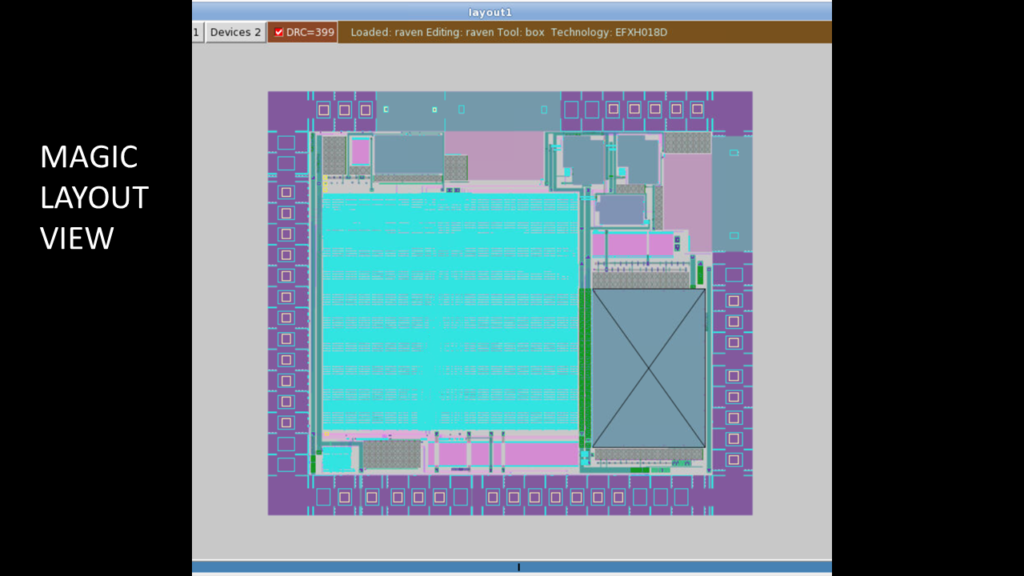
Now that it’s clear, that we can tapeout using open-source EDA tools (referring to recent RavenSoC tapeout by Efabless Corp. Pvt. Ltd. using XFAB 180nm technology node, see above pic), I think there will be more and more people using these tools, especially students, who can now learn entire VLSI backend using opensource EDA tools.

Now there will be lot of queries, so I thought of starting FAQ section for everyone who will be using MAGIC VLSI Layout tool. These are real-time LIVE conversations, which many people have emailed to me and Tim Edwards (SVP of Analog Platform, Efabless Corp. Pvt. Ltd.), and we have been consistently replying them. Hope you find them useful. Will be adding more FAQ’s in upcoming days

Question) Why doesn’t psubstratecontact and nsubstratecontact, which are defined in below ’tile’ section of tech file, appears in ‘contact’ section of tech file?

active  psubstratepcontact,pohmiccontact,poc,pwcontact,pwc,psc

active  nsubstratencontact,nohmiccontact,noc,nwcontact,nwc,nsc

Answer) Don’t they?  The standard scmos.tech file has:

nsc nsd metal1
psc psd metal1

Sometimes it’s hard to see because magic uses all these aliases for names. If you have a techfile that’s missing something from the contact section, it’s possible to define a contact just with the
connectivity (i.e., in the “connect” section).  The main difference is that the “contact” section handles all the varieties of the paint/erase tables.  A contact defined without using “contact” will have all sorts of strange behavior when you select it and start moving or stretching it, or deleting it.

Question) I see in tech file, the tile type psd is “psubstratepdiff” and nsd is “nsubstratendiff”

active  psubstratepdiff,pohmicdiff,pod,ppdiff,ppd,psd

active  nsubstratendiff,nohmicdiff,nod,nndiff,nnd,nsd

Is it an overlap tile between “psubstrate and ndiff” and “nsubstrate and pdiff”?

Shouldn’t it be psd = psubstratendiff and nsd = nsubstratepdiff ?

Answer) No, psd is pdiff in psubstrate (i.e., P+) and nsd is ndiff in nwell (i.e., N+).  These are the traditional names in scmos.tech.  I also find them confusing and think that they should just be called “pplus” and “nplus”. I have not heard anyone use the term “ohmic diffusion” outside of Magic
techfiles and documentation, that I recall.

Question) Ok

So in a twin-tub CMOS process, ‘nsd’ and ‘psd’ are the ‘tubs’ or ‘wells’ inside which we build nmos/pmos, right?

Naming convention is confusing, as I haven’t heard of ‘ndiff’ in ‘nwell’ or ‘pdiff’ in psubstrate. Its the other way round in fabrication, right?

Answer) Part of the confusion is because most layout editors, because they have a very mask-centric representation, only show “active”, and then have other boxes representing “wells” and “implants”.  Magic is different because it likes to show a more functional view, and sometimes you don’t
see the mask layers at all.  Implant layers (P+ implant, N+ implant) are usually not shown.  Instead, there are four kinds of diffusion shown:

“pdiff”    is diffusion with P+ implant inside N-well
“ndiff”    is diffusion with N+ implant in P-substrate (or P-well)
“psd”      is diffusion with P+ implant in P-substrate (or P-well)
“nsd”      is diffusion with N+ implant inside N-well.

So “psd” is the P-substrate (or P-well) tap, usually tied to ground, and “nsd” is the N-well tap, usually tied to VDD.

A twin-tub process may or may not show “pwell” explicitly, as the mask may be defined as (NOT nwell).  By having different types for “ndiff” and “pdiff”, magic allows a layout to be drawn with no wells at all—it will figure out where the wells are from where the ndiff and pdiff are, and automatically generate them (I might also add that this is dangerously prone to error, and nobody does it that way).

All above conversation and many more has been captured in a more structured form, in my below online course:

https://www.udemy.com/vlsi-academy-custom-layout/?couponCode=FAQ_MAGIC

Look for more FAQ’s coming up…All the best and happy learning….

Registration for Ethical RISC-V IoT Workshop

Welcome to Ethical RISC-V IoT Workshop

The “Ethical RISC-V IoT Workshop” at IIIT Bangalore, organized in collaboration with VSD, is a structured, educational competition aimed at exploring real-world challenges in IoT and embedded systems. Participants progress through three stages: building an application, injecting and managing faults, and enhancing application security. The event spans from May 9 to June 15, 2024, culminating in a showcase of top innovations and an award ceremony. This hands-on hackathon emphasizes learning, testing, and securing applications in a collaborative and competitive environment.

Rules :
  1. Only for Indian Student whose college is registered under VTU
  2. Only team of 2 members can Register
  3. Use only VSDSquadron Mini resources for product development
Awards :
  1. Prize money for final 10 Team
  2. 3 Winner team’s Product will be evaluated for Incubation
  3. 7 consolation prizes
  4. Completion Certificate to final round qualifier
  5. Chance to build a Proud Secured RISC-V Platform for India

Date for Registration : 9th May - 22nd May, 2024
Hackathon Inauguration : 23rd May 2024

VSDSquadron (Educational Board)

VSDSquadron, a cutting-edge development board based on the RISC-V architecture that is fully open-source. This board presents an exceptional opportunity for individuals to learn about RISC-V and VLSI chip design utilizing only open-source tools, starting from the RTL and extending all the way to the GDSII. The possibilities for learning and advancement with this technology are limitless.

Furthermore, the RISC-V chips on these boards should be open for VLSI chip design learning, allowing you to explore PNR, standard cells, and layout design. And guess what? vsdsquadron is the perfect solution for all your needs! With its comprehensive documentation and scalable labs, thousands of students can learn and grow together.

VSD HDP (Hardware Design Program) Duration-10 Week

With VSD Hardware Design Program (VSD-HDP),  you have the opportunity to push the boundaries of what exist in open source and establish the new benchmark for tomorrow.

It will leverage your degree in Electrical or Computer Engineering to work with

  • Programmable logic
  • Analog/ digital IP
  • RISC-V
  • Architecture & microprocessors
  • ASICs and SoCs on high-density digital or RF circuit cards
  • Gain hands-on knowledge during design validation and system integration.

Sounds exciting to just get started with expert mentors, doesn’t it? But we are looking for the next generation of learners, inventors, rebels, risk takers, and pioneers.

“Spend your summer working in the future !!”

Outcomes of VSD Online Research IP Design Internship Program

  1. Job opportunities in Semiconductor Industry
  2. Research work can be submitted to VLSI International journals
  3. Participate in Semiconductor International Conference with Internship Research Work
  4. Paper Publications in IEEE Conference and SIG groups
  5. Tape out opportunity and IP Royalty
  6. Interact with world class Semiconductor designer and researchers
  7. Academic professions where more research projects are encouraged.
  8. All the above research and publication work will help colleges and institutes to improve accreditation levels.

Know More Information

VSD – Intelligent Assessment Technology (VSD-IAT)

VSD – Intelligent Assessment Technology (VSD-IAT) is expertly built training platform and is suited for designer requirements. Semiconductor companies understand the value of training automation and Engineer performance enhancement, and do not need to be convinced of the impact of a virtual platform for learning. VSD trainings are quick, relevant, and easy to access from any device at any time zone.

VSD Intern Webinars

VSD Interns made it happen !!

VSD is working towards creating innovative talent pool who are ready to develop design and products for the new tech world. VSD believes in “Learning by doing principle” , and always prepare the student to apply the knowledge learned in the workshops, webinars and courses. We always push our students to work on new designs, test it and work continuously till it becomes the best performing design. Any student who enrolls to VSD community starts working with small design and grows with us and develops a tapeout level design with complete honesty and dedication towards the Work !!

Check out VSD Interns Achievement!

VSDOpen Online Conference

Welcome to the World’s only online conference in Semiconductor Industry VSDOpen Conference. With enormous support and global presence of audience from different segments of industrial lobby and academia made a highly successful event. Evolution is change in the genetic makeup of a population over time, online conference is one kind evaluation everyone adapt soon. 

  • VSDOpen 2022 is an online conference to share open-source research with the community and promote  hardware design mostly done by the student community.
  • VSDOpen 2022 is based on the theme “How to lower the cost to learn, build, and tapeout chips ?”  , which will provide a platform to community to build stronger designs and strengthen the future of Chip design.
  • VSDOpen is envisioned to create a community based revolution in semiconductor hardware technology.
  • The open source attitude is required to bring out the talent and innovation from the community who are in remote part of world and have least access to the technologies.  And now Google support will help to bring the vision to execution by VSD team

VSD Online Course by Kunal Ghosh

VSD offers online course in complete spectrum of vlsi backend flow from RTL design, synthesis and Verification, SoC planning and design, Sign-off analysis, IP Design, CAD/EDA automation and basic UNIX/IT, Introduction to latest technology – RISC-V, Machine intelligence in EDA/CAD, VLSI Interview FAQ’s.

Current Reach – As of 2021, VSD and its partners have released 41 online VLSI courses and was successfully able to teach  ~35900 Unique students around 151 countries in 47 different languages, through its unique info-graphical and technology mediated learning methods.

Enquiry Form