Emphasizes hands-on learning and end-to-end chip development
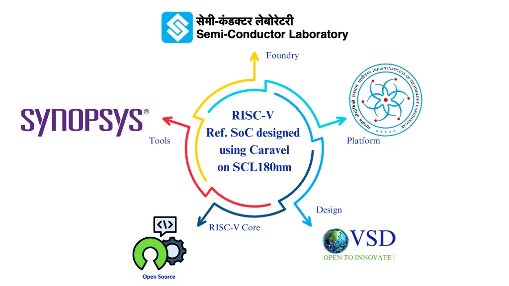
This project delivers a complete, hands-on journey to design, implement, and fabricate a RISC-V System-on-Chip (SoC) using Synopsys EDA tools and the SCL180 PDK. It’s crafted for students, educators, and professionals aiming to master end-to-end chip development—from RTL design to post-silicon validation. The RISC‑V Reference SoC Tapeout Program is a national-level initiative to empower engineering students with the most authentic VLSI experience—right from RTL design to actual silicon fabrication (tapeout). This program is part of India’s Semiconductor Mission to create skilled silicon designers who don’t just simulate—but fabricate. It brings together students, academic institutions, and national foundries to drive the next wave of innovation in VLSI.
Program Vision
Create a scalable and replicable reference tapeout program that can serve as a national framework for colleges and universities across India. This initiative focuses on building a proven, reusable methodology—from design to silicon—that academic institutions can adopt to execute their own production‑grade RISC‑V Reference SoC Tapeout Program using industry‑standard tools and PDKs.
Program Description
This 20‑week program demonstrates a complete tapeout cycle for a RISC‑V Reference SoC using Synopsys tools and the SCL180 nm PDK. It establishes an end‑to‑end flow—from RTL to GDSII and post‑silicon validation—combining online training with physical execution at IIT Gandhinagar (IITGN). The outcome is a reusable, documented flow that sets the standard for academic silicon tapeouts in India.
| Week | Dates | Theme | Hands‑on Labs (tool‑only) | Deliverables / Checkpoints |
|---|---|---|---|---|
| 1 | Thu, 18 Sep 2025 – Wed, 24 Sep 2025 | Environment + RTL sim basics | Set up toolchain; run iverilog simulations; inspect signals in GTKWave; inject a small RTL bug and detect via sim | iverilog run logs; 2 annotated GTKWave screenshots; 5–7 lines on the bug & fix |
| 2 | Thu, 25 Sep 2025 – Wed, 01 Oct 2025 | Synthesis & GLS | Synthesize with Yosys; Gate‑level simulation (GLS) with std‑cell models; compare RTL vs GLS behavior | Pre/post‑synth sim match screenshots; Yosys stat area/cell snippet; note on an observed optimization |
| 3 | Thu, 02 Oct 2025 – Wed, 08 Oct 2025 | RISC‑V ISA & toolchain | Build & run a small RISC‑V program (riscv‑gnu‑toolchain); simulate CPU testbench with iverilog + GTKWave (fetch/decode) | Waves showing PC, instruction, decode outputs; brief note on pipeline stage boundaries |
| 4 | Thu, 09 Oct 2025 – Wed, 15 Oct 2025 | Pipeline bugs, clock gating & CPU GLS | Reproduce a load‑use hazard; apply clock‑gating variant; re‑synthesize (Yosys); CPU‑level GLS with cell models | Waveforms: buggy vs fixed; one slide on toggle reduction with clock gating; GLS pass log snippet |
| 5 | Thu, 16 Oct 2025 – Wed, 22 Oct 2025 | STA fundamentals | Write core timing constraints (SDC); run OpenSTA on post‑synth netlist; identify worst setup/hold paths & constraint gaps | Setup/Hold report excerpts (WNS/TNS); 5–8 lines justifying clocks/IO delays/false or multicycle paths |
| 6 | Thu, 23 Oct 2025 – Wed, 29 Oct 2025 | CMOS & SPICE with SKY130 | Draw basic gates in Xschem; simulate in ngspice; sweep VDD/Temp/Load; extract rise/fall delays | 3 plots (delay vs load; delay vs VDD; rise vs fall); one‑pager explaining PVT effects on delay |
| 7 | Thu, 30 Oct 2025 – Wed, 05 Nov 2025 | OpenLane: floorplan → placement | Run OpenLane through floorplan & placement; tune utilization/aspect; tap/decap insertion; check congestion metrics | Floorplan/placement metrics snapshot; congestion heatmap/metrics; note on best util/aspect found |
| 8 | Thu, 06 Nov 2025 – Wed, 12 Nov 2025 | CTS, routing & post‑route STA | OpenLane: CTS → global/detail route; OpenSTA post‑CTS & post‑route; review hold fixes | Post‑route timing summary (WNS, TNS) at TT; final routed layout screenshot; note on hold‑fix strategy |
| 9 | Thu, 13 Nov 2025 – Wed, 19 Nov 2025 | Multi‑corner timing + sign‑off | Multi‑corner OpenSTA (slow/typ/fast); generate SDF and run SDF‑annotated GLS; assemble sign‑off artifacts | Table of WNS/TNS across corners; SDF‑GLS pass log & wave snapshot; list of sign‑off artifacts |
| 10 | Thu, 20 Nov 2025 – Wed, 26 Nov 2025 | Final polish & documentation | Re‑run best config to clean violations; summarize RTL→GDS flow, constraints, corner timing; short walkthrough video | Final timing & DRC status summary; 4–6 page PDF report; 2–3 min demo video link |
| Week | Dates | Theme | Hands‑on Labs (tool‑only) | Deliverables / Checkpoints |
|---|---|---|---|---|
| 1 | Wed, 10 Dec 2025 – Tue, 16 Dec 2025 | Fix SDC & make Housekeeping synthesizable | Repair SDC header/vars; place read_sdc before compile; add create_clock, set_clock_groups -asynchronous, IO delays; set_false_path & set_disable_timing for ring‑osc/analog arcs; de‑tri‑state internals; guard SIM‑only code; synthesize Housekeeping standalone then top | Clean vsdcaravel.sdc; updated Housekeeping RTL (no internal Zs); DC reports (clocks/QoR/timing); post‑synth netlists (HK + Top) |
| 2 | Wed, 17 Dec 2025 – Tue, 23 Dec 2025 | POR & SRAM macro plan + Hybrid GLS | Thin SCL POR/SRAM wrappers with USE_POWER_PINS; link macro .db/.lib in DC; mark dont_touch; provide SIM models; Hybrid GLS (GL for most; RTL for HK if needed); extend DV (UART, GPIO dir, Wishbone R/W, reset robustness); generate VCD/SAIF from RTL; rerun DC power with SAIF | POR/SRAM wrappers; updated DC link library & dont_touch; hybrid GLS script & passing logs; SAIF/VCD artifacts & updated power report |
| 3 | Wed, 24 Dec 2025 – Tue, 30 Dec 2025 | Full GLS (no black‑boxes) + STA convergence | Replace HK RTL with synthesized netlist; include SDF as available; integrate SRAM/POR models in GLS; cut non‑digital arcs in STA; firmware smoke (mgmt core fetch, minimal CSR poke); tighten SDC (generated clocks, strap case‑analysis, IO loads); fix top violators; iterate simple ECOs | Full‑GLS waves + pass logs (HK, UART, GPIO, WB, boot); updated SDC; timing reports (top 100 paths) per iteration |
| 4 | Wed, 31 Dec 2025 – Tue, 06 Jan 2026 | Sign‑off‑style STA & Handover | Final STA (setup/hold across corners; CDC review); final power with SAIF; DRC hygiene; reproducibility (make synth/gls/sta with docs) | STA pack (SDC + timing/power reports); GLS pack (scripts, pass logs, SDF list); Repro README + Make/Tcl entrypoints; closure slides |
| Week | Dates | Theme | Hands‑on Labs (tool‑only) | Deliverables / Checkpoints |
|---|---|---|---|---|
| 1 | Sat, 17 Jan 2026 – Fri, 23 Jan 2026 | PnR bring‑up, floorplan & pads | Freeze pad ring with SCL IO (ESD/corners/VDD/VSS); seal‑ring/scribe; floorplan (die/core, 55–65% util); place macros + halos; multi‑rail audit; level shifters if needed; PG grid; import clean SDC from GLS | Floorplan DEF/FP; pad ring + seal ring; PDN Tcl & tap/decap recipe; pinout CSV (bond map draft) |
| 2 | Sat, 24 Jan 2026 – Fri, 30 Jan 2026 | Placement & pre‑CTS timing | Insert tie/spare cells; global placement & legalization; clock plan (roots, skew target, buffer list); pre‑CTS opt: fix max tran/cap/fanout; pipeline/resize if needed; early RC (global route) for realistic timing | Placed DEF; pre‑CTS timing (max/min); congestion & utilization reports |
| 3 | Sat, 31 Jan 2026 – Fri, 06 Feb 2026 | CTS, post‑CTS timing & SI | Run CTS (balanced/useful skew); post‑CTS hold fixing; RC‑aware re‑opt (size/buffer); crosstalk mitigation; STA across TT/SS/FF | Post‑CTS DEF; timing (setup/hold, clock summary); clock QoR (insertion, skew, buffer count) |
| 4 | Sat, 07 Feb 2026 – Fri, 13 Feb 2026 | Route, antenna, fill, draft DRC/LVS | Global + detailed route; antenna check/fix (diodes/jumps) & ECO route; metal density fill/slotting; first full‑chip DRC; prep LVS | Routed DEF/GDS; antenna & density reports; first DRC/LVS logs |
| 5 | Sat, 14 Feb 2026 – Fri, 20 Feb 2026 | Sign‑off PEX, STA, IR/EM, GLS/FEV | Golden PEX → SPEF; sign‑off STA (all PVT + OCV/AOCV) & ECO; IR/EM; reinforce PG if needed; post‑layout GLS with SDF; formal equivalence | SPEF/SDF; sign‑off STA pack; IR/EM reports; GLS pass logs; FEV clean report |
| 6 | Sat, 21 Feb 2026 – Fri, 27 Feb 2026 | Tapeout kit & submission | Final DRC/LVS = 0 (or approved waivers); re‑fill after ECOs and re‑DRC; build tapeout package (GDSII, layer map, tech notes, netlist, LEF, reports, waivers); SCL jobdeck/forms; top‑cell checks; bonding/package kit & pinout CSV; golden re‑runs | Submission archive (GDSII + docs) & checklist; bonding/package kit |
Registration will close in
VSDSquadron was launched by Prof. V. Kamakoti, Director of IIT Madras
VSD Launches VSDSquadron In Collaboration With IIT Madras & DIR-V

Job Roles, Convergence With Embedded Systems, and Startups
VSD showcased at Semicon India 2023

VSDSquadron Educational board on Tamil News channel
5 Day Workshop on VLSI Design Flow using RISCV and EDA Tools
Karnataka VLSI roadshow at Sahyadri College, Mangalore
Welcome to Ethical RISC-V IoT Workshop
The “Ethical RISC-V IoT Workshop” at IIIT Bangalore, organized in collaboration with VSD, is a structured, educational competition aimed at exploring real-world challenges in IoT and embedded systems. Participants progress through three stages: building an application, injecting and managing faults, and enhancing application security. The event spans from May 9 to June 15, 2024, culminating in a showcase of top innovations and an award ceremony. This hands-on hackathon emphasizes learning, testing, and securing applications in a collaborative and competitive environment.
VSDSquadron, a cutting-edge development board based on the RISC-V architecture that is fully open-source. This board presents an exceptional opportunity for individuals to learn about RISC-V and VLSI chip design utilizing only open-source tools, starting from the RTL and extending all the way to the GDSII. The possibilities for learning and advancement with this technology are limitless.
Furthermore, the RISC-V chips on these boards should be open for VLSI chip design learning, allowing you to explore PNR, standard cells, and layout design. And guess what? vsdsquadron is the perfect solution for all your needs! With its comprehensive documentation and scalable labs, thousands of students can learn and grow together.
With VSD Hardware Design Program (VSD-HDP), you have the opportunity to push the boundaries of what exist in open source and establish the new benchmark for tomorrow.
It will leverage your degree in Electrical or Computer Engineering to work with
Sounds exciting to just get started with expert mentors, doesn’t it? But we are looking for the next generation of learners, inventors, rebels, risk takers, and pioneers.
“Spend your summer working in the future !!”
Outcomes of VSD Online Research IP Design Internship Program
VSD – Intelligent Assessment Technology (VSD-IAT) is expertly built training platform and is suited for designer requirements. Semiconductor companies understand the value of training automation and Engineer performance enhancement, and do not need to be convinced of the impact of a virtual platform for learning. VSD trainings are quick, relevant, and easy to access from any device at any time zone.
VSD is working towards creating innovative talent pool who are ready to develop design and products for the new tech world. VSD believes in “Learning by doing principle” , and always prepare the student to apply the knowledge learned in the workshops, webinars and courses. We always push our students to work on new designs, test it and work continuously till it becomes the best performing design. Any student who enrolls to VSD community starts working with small design and grows with us and develops a tapeout level design with complete honesty and dedication towards the Work !!
Check out VSD Interns Achievement!
Welcome to the World’s only online conference in Semiconductor Industry VSDOpen Conference. With enormous support and global presence of audience from different segments of industrial lobby and academia made a highly successful event. Evolution is change in the genetic makeup of a population over time, online conference is one kind evaluation everyone adapt soon.
VSD offers online course in complete spectrum of vlsi backend flow from RTL design, synthesis and Verification, SoC planning and design, Sign-off analysis, IP Design, CAD/EDA automation and basic UNIX/IT, Introduction to latest technology – RISC-V, Machine intelligence in EDA/CAD, VLSI Interview FAQ’s.
Current Reach – As of 2021, VSD and its partners have released 41 online VLSI courses and was successfully able to teach ~35900 Unique students around 151 countries in 47 different languages, through its unique info-graphical and technology mediated learning methods.
