IP Overview
The SPI Master IP (Mode-0) is a memory-mapped peripheral designed for the VSDSquadron RISC-V SoC. It enables communication with external SPI-compatible devices using SPI Mode-0 timing.
Typical Use Cases
- SPI sensors (IMU, temperature, ADC)
- SPI Flash memory
- DAC / ADC devices
- Expansion header peripherals
Why Use This IP
- Provides deterministic SPI timing in hardware
- Reduces software complexity compared to bit-banging
- Simple register-based control model
- Plug-and-play integration with VSDSquadron SoC
Feature Summary
- SPI Master operation
- SPI Mode-0 (CPOL=0, CPHA=0)
- 8-bit full-duplex transfer
- Single slave select
- Programmable clock divider
- Polling-based status control
Clock Assumptions
- Uses system clock
clk - SPI clock derived from programmable divider
Limitations
- Only Mode-0 supported
- Single SPI slave
- No interrupts
- No FIFO support
Block Diagram
The following block diagram shows the logical structure of the SPI Master IP and its interaction with the RISC-V CPU and external SPI device.
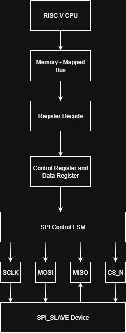
Block Description
- Register Decode
Decodes memory-mapped accesses from the CPU and selects SPI registers. - Control Registers
Hold enable, start, clock divider, and transmit data. - SPI Control FSM
Generates SPI clock, controls chip-select, shifts data, and captures received bits. - SPI Signals
Standard SPI Master signals connected to an external peripheral.
Hardware Usage
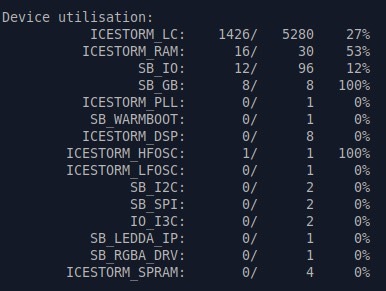
Terms
- ICESTORM_LC – Logic Cell Usage
- ICESTORM_RAM – BRAM Usage
- ICESTORM_HFOSC – Internal High Frequency Oscillator
- SB_IO – FPGA Pins Usage
- SB_GB – Global Buffer Usage
Key Observation
- SoC frequency – 12 MHz , produced by internal oscillator
- ALU and Counters are optimised using carry chains.
- 100% utilization of Global Buffer suggests we cannot add extra clock domains
RTL And Register Map
SPI Master IP Module is built seperatln and instantiated in SoC Module. You can find the RTL Code for SPI Master IP below
SPI Master IP RTL
module SPI(
//Global clk and rst
    input clk,
    input rst,
//Control and data signals
    input sel,
    input w_en,
    input r_en,
    input [31:0] wdata,
    output reg [31:0] rdata,
    input [1:0] offset,
//SPI Master signals
    output reg sclk,
    output reg mosi,
    input miso,
    output reg cs_n
    );

//register file
localparam CNTRL=2'b00;
localparam TXDATA=2'b01;
localparam RXDATA=2'b10;
localparam STATUS=2'b11;

//control register fields
reg en;
reg start;
reg [7:0]clkdiv;

//status reg
reg busy;
reg done;

//counter for clkddivider
reg [7:0]clk_cnt;


//bit counter for transfering 8 bits
reg [2:0]bit;

//Data registers
reg [7:0]tx;
reg [7:0]rx;
reg [7:0]rxdata; //rx data will be stored in done phase to avoid corruption
//REGISTER write
always @(posedge clk) begin
    if(rst) begin
        en<=0;
        start<=0;
        clkdiv<=0;
        bit<=0;
        busy<=0;
        done<=0;
        clkdiv<=0;
        tx<=0;
        rx<=0;
        rxdata<=0;
        end

     else if(sel && w_en) begin
        case(offset)
            CNTRL: begin en<=wdata[0];
                            clkdiv<=wdata[15:8];
                            if(~busy)
                                start<=wdata[1];
                   end
            TXDATA: begin tx<=wdata[7:0];
                    end
            STATUS: begin if(wdata[1])
                            done<=0;
                    end
         endcase
      end
end

//FSM
reg [1:0]state;

localparam IDLE=2'b00;
localparam  DATA_STATE=2'b01;
localparam DONE=2'b10;


always @(posedge clk) begin
    if(rst) begin
            state   <= IDLE;
            sclk    <= 1'b0;
            cs_n    <= 1'b1;
            mosi    <= 1'b0;
            busy    <= 1'b0;
            done    <= 1'b0;
            clk_cnt <= 8'd0;
            bit <= 3'd0;
            rx<= 8'd0;
            rxdata  <= 8'd0;
        end


     else begin
        case(state)
            IDLE:begin sclk<=1'b0;
                        cs_n<=1'b1;
                        busy<=1'b0;
                        if(en && start && ~busy) begin
                            cs_n<=1'b0;
                            busy<=1'b1;
                            clk_cnt<=8'd0;
                            bit<=3'd7;
                            mosi<=tx[7];
                            rx<=0;
                            done<=1'b0;
                            state<=DATA_STATE;
                         end
                   end
      DATA_STATE: begin if(clk_cnt == clkdiv)begin
                            clk_cnt<=8'd0;
                            sclk<=~sclk;
                          //Sample MISO at falling eddge according to mode 0
                            if(sclk == 1'b0)
                                rx<={rx[6:0],miso};
                         //Shift at Rising Edge
                            else begin
                                    if(bit != 0) begin
                                        bit<=bit - 1;
                                        mosi<=tx[bit - 1];
                                    end
                                    else state<=DONE;
                            end
                         end
                         else clk_cnt<=clk_cnt + 1;
                    end
            DONE: begin cs_n<=1'b1;
                        sclk<=1'b0;
                        busy<=1'b0;
                        done<=1'b1;
                        rxdata<=rx;
                        state<=IDLE;
                    end
         default: state<=IDLE;
        endcase
    end
end

//READ
always @(*) begin
    if(sel && r_en) begin
        case(offset)
            CNTRL: rdata = {16'd0,clkdiv , 6'd0, start, en};
            TXDATA: rdata = {24'd0, tx};
            RXDATA: rdata = {24'd0,rxdata};
            STATUS: rdata = {29'd0, 1'b1, done, busy};
            default: rdata= 32'b0;
         endcase
      end
end
endmodule
Use the following instantiation template inside the SoC top:
wire [31:0] spi_rdata;

SPI SPI (
  .clk      (clk),
  .rst      (!resetn),
  .sel      (isIO & mem_addr[12]),
  .w_en     (mem_wstrb),
  .r_en     (mem_rstrb),
  .offset   (mem_addr[3:2]),
  .wdata    (mem_wdata),
  .rdata    (spi_rdata),

  // SPI pins
  .sclk     (sclk),
  .mosi     (mosi),
  .miso     (miso),
  .cs_n     (cs_n)
);
The SoC Has the instantiated IP ,so there is are no changes required for this file. It can be directly use to Generate Bitstream after download. All requied dependencies are provide in /RTL.
Register Map
Address Mapping
SPI IP is selected when:
mem_addr[22] == 1(IO space)mem_addr[12] == 1(SPI offset)
SPI IP base address: 0x00401000
Register Summary
| Offset | Register | R/W | Description |
|---|---|---|---|
| 0x00 | CTRL | R/W | Enable, start, clock divider |
| 0x04 | TXDATA | R/W | Transmit data |
| 0x08 | RXDATA | R | Received data |
| 0x0C | STATUS | R/W | Busy and done flags |
CTRL Register (0x00)
| Bits | Name | Access | Description |
|---|---|---|---|
| 0 | EN | R/W | Enable SPI |
| 1 | START | R/W | Start transfer |
| 15:8 | CLKDIV | R/W | SPI clock divider |
| Others | – | – | Reserved |
Reset value: 0x00000000
TXDATA Register (0x04)
| Bits | Name | Access | Description |
|---|---|---|---|
| 7:0 | TX | R/W | Transmit byte |
RXDATA Register (0x08)
| Bits | Name | Access | Description |
|---|---|---|---|
| 7:0 | RX | R | Received byte |
STATUS Register (0x0C)
How to Use IP
1. Create a C program with address mapping file included Or use a Pre made C Program SPI_MASTER.
2. Convert it to .hex file using command
cd Firmware/
make SPI_MASTER.bram.hex
The make file copies your Hex file to firmware.h in your RTL folder.
3. Generating Bitstream
cd ..
cd RTL/
make build
4. Flash to your FPGA
make flash5. To check UART output
make terminalPins
| Interface | Signal | Direction | FPGA Pin | Notes |
|---|---|---|---|---|
| Clock | CLK | Input | 28 | System clock input |
| Reset | RESET | Input | 10 | Active-high reset input |
| UART | TXD | Output | 4 | UART transmit (FPGA → PC) |
| UART | RXD | Input | 3 | UART receive (PC → FPGA) |
| GPIO LEDs | GPIO[0] | Input/Output | 38 | Digital GPIO 0 |
| GPIO LEDs | GPIO[1] | Input/Output | 43 | Digital GPIO 1 |
| GPIO LEDs | GPIO[2] | Input/Output | 45 | Digital GPIO 2 |
| GPIO LEDs | GPIO[3] | Input/Output | 47 | Digital GPIO 3 |
| GPIO LEDs | GPIO[4] | Input/Output | 6 | Digital GPIO 4 |
| SPI | sclk | Output | 34 | SPI clock |
| SPI | mosi | Output | 35 | SPI MOSI |
| SPI | miso | Input | 36 | SPI MISO |
| SPI | cs_n | Output | 37 | SPI chip select (active low) |
Demo
LED Order (From left)
- LED 1 – CS_N
- LED 2 – MOSI
- LED 3 – SCLK
The above Program is running in a loop, hence when reset is clicked CS_N goes to logic state 1. Later to Logic 0 indicating that slave is selected.
SCLK frequency is 23.5 KHz
UART Output
— SPI MASTER IP TEST (MODE-0) —
A5->XX
A5->XX
A5->XX
